
PCB production process: cut - drilling – copper immersion – pressure film – exposure – development – electro-copper – electro-tin – film removal – etching – Retinning – optical inspection – printing soldermask – solder resist exposure, development – characters - surface treatment – moulding – electrical testing – final inspection – sampling – packaging. Specifically as follows:
1. Cut
The original copper-clad board cut into boards that can be used in the SMT production line production process
2. Drilling
So that the PCB board layer to layer through holes, in order to achieve the purpose of connecting layers.
3. Copper immersion
After drilling the circuit board in the copper immersion cylinder will occur redox reaction, the formation of copper layer on the holes for hole metallisation, so that the original insulating substrate surface deposition of copper, to achieve interlayer electrical communication.
4. Pressure film
Pressure film after the PCB above the pressure of a layer of blue dry film, dry film is a carrier, in the circuit process is very important. Dry film compared to wet film, with higher stability and better quality, can directly do non-metallised through-hole.
5. Exposure
Align the negative with the substrate of the pressed dry film, and use ultraviolet light in the exposure machine to transfer the negative to the light-sensitive dry film.
6. Development
The use of weak alkaline developer solution has not been exposed to the dry film or wet film dissolved rinse off, retaining the part that has been exposed.
7. Electro - copper
PCB into the electro-copper equipment, copper part of the copper was electrified on the copper, the dry film blocked the part of the reaction is not!
8. Electro – tin
Purpose is to remove that part of the copper protected by the dry film to do the preparatory work.
9. Film removal
Will protect the copper surface has been exposed to the dry film with sodium hydroxide solution stripped off, revealing the line graphics.
10. Etching
Has not been exposed to the dry film or wet film by the developer to remove the copper surface will be exposed, with acidic copper chloride will be exposed to this part of the copper surface of the dissolution of the corrosion of the line to get the desired line.
11. Retinning
Retinning is the use of retinning water to retire the tin on the line, so that the line back to the original colour of copper.
12. Optical inspection
There are generally two detection methods, one is to observe with the naked eye, the second is to use optical AOI. AOI working principle is to use high-definition image camera for rapid shooting, and then use the picture taken with the original file for comparison, can be a fundamental solution to the occurrence of open and short circuits, and micro-open, micro-short, and other hidden dangers.
13. Printing soldermask
Solder resist is one of the most critical processes in the production of printed circuit boards, mainly through screen printing or coating solder resist ink, coated with a layer of solder resist on the surface of the board, through the exposure of the development, revealing to be welded to the plate and the hole, and other places covered with a layer of solder resist to prevent short-circuiting when welding
14. Solder resist exposure, development
The purpose of the solder resist is to remove solder resist from the weld pads and other places. First solder resist film on the board covered with green oil, film (to open the window of the place is black, do not open the window of the place is transparent), and then placed in the exposure machine for exposure, to open the window of the part of the film, because the film is black, black blocked the light was not exposed, with the solder resist green oil state changes, part of the green oil was exposed, part of the green oil was not exposed to the green oil, from the surface of the From the surface, this time is still green.
15. Characters
The desired text, trademarks, parts and other symbols, printed in the form of stencil printing on the PCB board surface, and then exposed to ultraviolet radiation on the board surface
16. Surface treatment
The purpose is to ensure good solderability or electrical properties. Common surface treatment: spray tin, immersion gold, OSP, immersion tin, immersion silver, nickel and palladium gold, electric hard gold, electric gold finger.
17. Moulding
Cut the PCB into the required form factor.
18. Electrical testing
Simulate the state of the circuit board, power on to check the electrical properties of open and short circuit.
19. Final inspection, sampling, packaging
The appearance of the PCB, size, aperture, board thickness, marking and so on one by one check to meet customer requirements. Qualified products will be packaged, easy to store and transport.
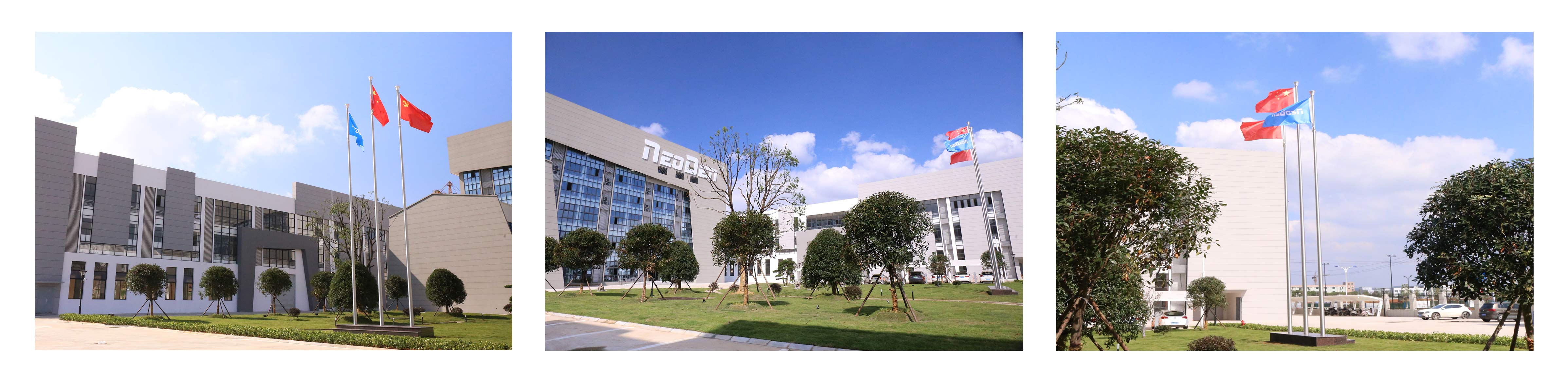
Company profile
Zhejiang NeoDen Technology Co., LTD., founded in 2010, is a professional manufacturer specialized in SMT pick and place machine, reflow oven, stencil printing machine, SMT production line and other SMT Products. We have our own R & D team and own factory, taking advantage of our own rich experienced R&D, well trained production, won great reputation from the world wide customers.
We are in a good position not only to supply you high quality pnp machine, but also the excellent after sales service.
Well-trained engineers will offer you any technical support.
25+ engineers powerful after-sales service team can respond customers queries and enquiries within 8 hours.
Professional solutions can be offered within 24 hours both workday and holidays.
Post time: Jul-22-2025