
Introduction
Amid the IoT wave, billions of devices—from smart home appliances to industrial sensors—are connecting to form a vast network. At the core of these devices lies the PCBA, which handles critical functions like computing, communication, and sensing. Consequently, the PCBA manufacturing process for IoT devices faces challenges and requirements distinctly different from traditional electronics. Thoroughly analyzing these critical issues is essential to ensuring the reliability and cost-effectiveness of IoT devices.
I. Key Challenges: Miniaturization, Low Power Consumption, and High Integration
1. Miniaturization and High-Density Assembly
IoT devices often require integration into confined spaces, such as smart wristbands, wireless earbuds, or micro-sensors. This demands highly compact PCBA designs with densely packed components, often utilizing smaller package sizes (e.g., 01005). This miniaturization trend imposes stringent demands on PCBA manufacturing processes: precision requirements for SMT placement machines, temperature control for reflow soldering machine, and manual rework complexity all increase exponentially. Even minor misalignments or soldering defects can cause entire PCBA failures.
2. Ultra-Low Power Design and Testing
To extend battery life, many IoT devices require ultra-low power consumption. This necessitates meticulous selection and placement of every component on the PCBA—from chips to resistors—to minimize current leakage. Post-manufacturing testing involves not only standard functional checks but also precise power consumption measurements to ensure current draw aligns with design specifications during both sleep and active states. The challenge here lies in accurately capturing microampere-level current fluctuations without disrupting normal device operation.
3. High Integration of Multiple Communication Technologies
IoT devices typically integrate various wireless communication technologies such as Wi-Fi, Bluetooth, Zigbee, and NB-IoT. The performance of these radio frequency (RF) circuits imposes stringent demands on PCB routing, component placement, and interference resistance. During PCBA manufacturing, even minor production deviations can disrupt antenna impedance matching, leading to weakened signal strength or unstable communication. Therefore, specialized RF test equipment is essential for comprehensive verification of the PCBA’s wireless performance.
II. Solutions: Optimizing PCBA Manufacturing Processes
1. Adopting High-Precision Automated Equipment
To address the challenges of miniaturization and high-density assembly, factories must invest in higher-precision pick and place machines, SMT stencil printers, and AOI (Automated Optical Inspection) equipment. These automated systems ensure precise component alignment and uniform solder paste application, thereby improving first-pass yield and reducing rework.
2. Implementing Dedicated Power Consumption Testing Platforms
Given the characteristics of low-power IoT devices, specialized power consumption testing platforms must be established. These platforms simulate device states across various operating modes, utilizing high-sensitivity current probes and oscilloscopes to precisely measure and analyze power consumption curves. This helps engineers identify potential power leakage points.
3. Strengthening RF Performance Testing
Post-PCBA manufacturing, RF performance testing is indispensable. Beyond conventional signal strength checks, spectrum analysis, harmonic testing, and immunity testing are required to ensure stable operation in complex electromagnetic environments. For PCBA with integrated antennas, antenna performance testing in an anechoic chamber is essential to validate radiation efficiency and pattern characteristics.
Conclusion
The proliferation of IoT devices is redefining standards in the PCBA manufacturing industry. It is no longer merely simple electronic component assembly but a systematic engineering endeavor integrating precision manufacturing, low-power design, and complex communication technologies. Only by addressing the challenges of miniaturization, low power consumption, and high integration—while optimizing manufacturing and testing processes—can PCBA factories provide a solid foundation for the reliability, cost-effectiveness, and market success of IoT devices.
Company Profile
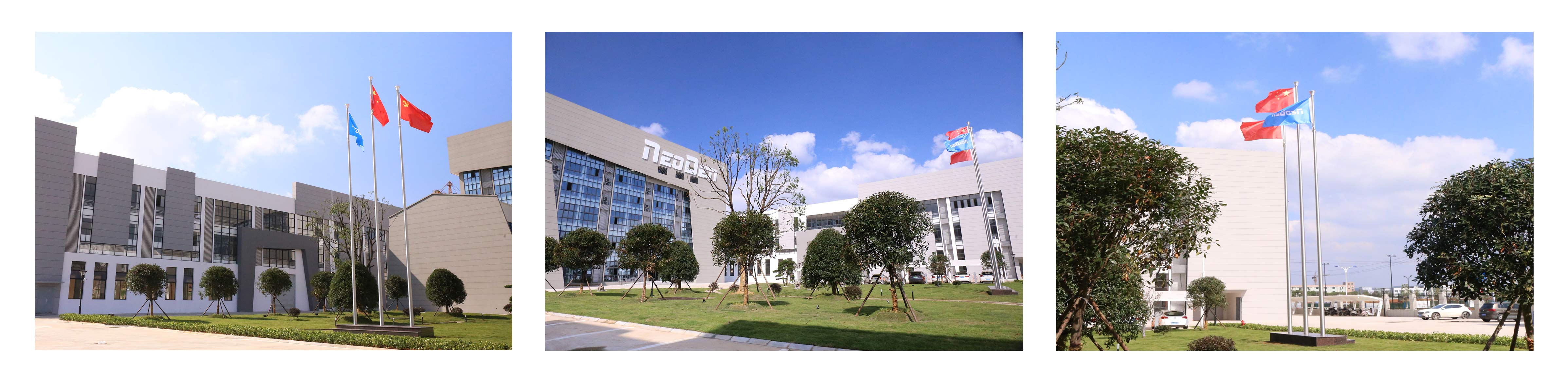
Zhejiang NeoDen Technology Co., Ltd. has been manufacturing and exporting various small pick and place machines since 2010. Taking advantage of our own rich experienced R&D, well trained production, NeoDen wins great reputation from the world wide customers.
In our global Ecosystem, we collaborate with our best partners to deliver a more
closing sales service, high professional and efficient technical support.
We believe that great people and partners make NeoDen a great company and that our commitment to Innovation, Diversity and Sustainability ensures that SMT automation is accessible to every hobbyist everywhere.
Post time: Sep-25-2025