
Introduction
The advent of the 5G era is reshaping our digital world at unprecedented speeds and connectivity levels. From ultra-high-definition video streaming and autonomous vehicles to industrial internet, the vision of an interconnected world is becoming reality. Behind this monumental technological transformation, the PCBA manufacturing industry—the core of electronic devices—faces a series of unprecedented challenges. These challenges extend beyond refining production techniques to fundamentally shape the future trajectory of the entire industry.
New Demands of 5G Technology on PCBA
To achieve high-speed, low-latency performance, 5G devices require increasingly complex and precise internal PCBA designs. These novel technical requirements pose significant tests to traditional PCBA manufacturing processes.
1. Challenges in High-Frequency, High-Speed Signal Processing
5G communication utilizes higher frequency bands (such as millimeter waves), significantly increasing signal transmission frequencies on PCBs. Traditional PCB materials and routing designs are prone to signal attenuation, crosstalk, and electromagnetic interference (EMI) in high-frequency environments. This necessitates the adoption of new high-frequency, high-speed PCB materials (e.g., polytetrafluoroethylene PTFE, hydrocarbon resins) in PCBA manufacturing. Strict impedance control during design and production is essential to ensure signal integrity. Even minor manufacturing defects can cause signal loss or distortion, compromising device communication performance.
2. Challenges of Miniaturization and High-Density Packaging
To meet the miniaturization and slimline requirements of 5G devices (such as smartphones and base stations), PCBA component packaging sizes are becoming increasingly smaller and denser. The use of ultra-micro components like 01005 and 008004 is growing commonplace, while high-density packaging such as BGA (Ball Grid Array) and LGA (Land Grid Array) has become standard. This not only imposes extremely high demands on SMT (Surface Mount Technology) placement accuracy but also makes solder joint quality control exceptionally challenging. Even the slightest solder deficiency or voids can cause circuit open circuits or short circuits, compromising product reliability.
3. New Challenges in Thermal Management and Power Control
5G chips generate substantial heat during high-speed operation and large-data transmission. Efficient thermal design is critical for maintaining device performance and extending lifespan. This necessitates integrating thermal solutions into PCBA design and manufacturing processes, such as incorporating thermal vias into PCBs, using metal-core boards, or employing heat-dissipating substrates. Simultaneously, the low-power requirements of 5G devices impose higher precision demands on the placement and testing of power management chips. Ensuring efficient thermal management and precise power control within extremely limited space presents a critical challenge PCBA manufacturers must overcome.
The Path to Technological Innovation in Addressing Challenges: Confronting the demands of 5G, the PCBA processing industry is actively pursuing technological innovation:
1. Advanced Equipment and Process Upgrades
To handle high-density packaging, factories must adopt higher-precision SMT machines, solder paste printers, and reflow ovens. For inspection, beyond traditional AOI, 3D-SPI (3D solder paste inspection) and AXI (automated X-ray inspection) are essential to ensure solder joint quality for micro-solder points and BGA packages.
2. Material and Technology Research
Manufacturers must collaborate closely with PCB material suppliers and component vendors to jointly research and develop new materials and packaging technologies suitable for high-frequency, high-speed communications. Simultaneously, stricter production process control standards must be established to meet the demanding precision requirements of the 5G era.
3. Deep Integration of Digitalization and Intelligence
By adopting Industrial IoT, big data analytics, and artificial intelligence technologies, factories can achieve real-time production line monitoring, data traceability, and intelligent decision-making. For instance, AI-driven AOI systems enable more accurate identification of minute defects on high-frequency signal boards, while big data analysis optimizes production parameters to enhance yield rates.
Conclusion
The 5G era presents immense development opportunities for the PCBA processing industry while posing unprecedented technical challenges. Only enterprises that dare to invest in advanced equipment, continuously pursue technological innovation, and embrace digital transformation will emerge as key enablers of the 5G world in this technological revolution.
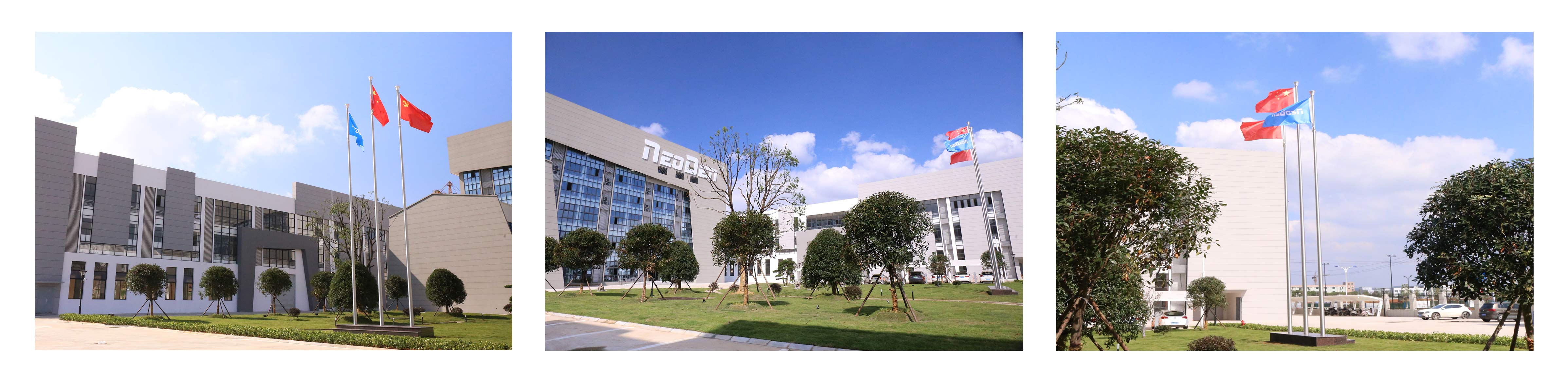
Quick facts about NeoDen
1) Established in 2010, 200 + employees, 27000+ Sq.m. factory.
2) NeoDen Products:Different Series PnP machines, NeoDen YY1, NeoDen4, NeoDen5, NeoDen K1830, NeoDen9, NeoDen N10P. Reflow Oven IN Series, as well as complete SMT Line includes all necessary SMT equipment.
3) Successful 10000+ customers across the globe.
4) 40+ Global Agents covered in Asia, Europe, America, Oceania and Africa.
5) R&D Center: 3 R&D departments with 25+ professional R&D engineers.
6) Listed with CE and got 70+ patents.
7) 30+ quality control and technical support engineers, 15+ senior international sales, for timely customer responding within 8 hours, and professional solutions providing within 24 hours.
Post time: Sep-18-2025