
Advanced packaging is one of the technological highlights of the ‘More than Moore’ era. As chips become increasingly difficult and expensive to miniaturise at each process node, engineers are putting multiple chips into advanced packages so that they no longer have to struggle to shrink them. This article provides a brief introduction to 10 of the most common terms used in advanced packaging technology.
2.5D packages
The 2.5D package is an advancement of traditional 2D IC packaging technology, allowing for finer line and space utilisation. In a 2.5D package, bare dies are stacked or placed side-by-side on top of an interposer layer with silicon via vias (TSVs). The base, or interposer layer, provides connectivity between the chips.
The 2.5D package is typically used for high-end ASICs, FPGAs, GPUs and memory cubes. 2008 saw Xilinx divide its large FPGAs into four smaller chips with higher yields and connect these to the silicon interposer layer. 2.5D packages were thus born and eventually became widely used for high bandwidth memory (HBM) processor integration.
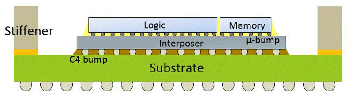
Diagram of a 2.5D package
3D packaging
In a 3D IC package, logic die are stacked together or with storage die, eliminating the need to build large System-on-Chips (SoCs). The die are connected to each other by an active interposer layer, while 2.5D IC packages use conductive bumps or TSVs to stack components on the interposer layer, 3D IC packages connect multiple layers of silicon wafers to components using TSVs.
TSV technology is the key enabling technology in both 2.5D and 3D IC packages, and the semiconductor industry has been using HBM technology to produce DRAM chips in 3D IC packages.
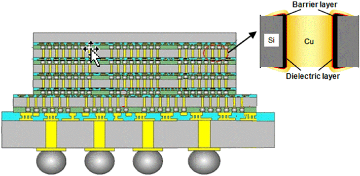
A cross-sectional view of the 3D package shows that the vertical interconnection between silicon chips is achieved through metallic copper TSVs.
Chiplet
Chiplets are another form of 3D IC packaging that enables the heterogeneous integration of CMOS and non-CMOS components. In other words, they are smaller SoCs, also called chiplets, rather than large SoCs in a package.
Breaking down a large SoC into smaller, smaller chips offers higher yields and lower costs than a single bare die. chiplets allow designers to take advantage of a wide range of IP without having to consider which process node to use and which technology to use to manufacture it. They can use a wide range of materials, including silicon, glass and laminates to fabricate the chip.
Chiplet-based systems are made up of multiple Chiplets on an intermediary layer
Fan Out Packages
In a Fan Out package, the “connection” is fanned off the surface of the chip to provide more external I/O. It uses an epoxy molding material (EMC) that is fully embedded in the die, eliminating the need for processes such as wafer bumping, fluxing, flip-chip mounting, cleaning, bottom spraying and curing. Therefore, no intermediary layer is required either, making heterogeneous integration much easier.
Fan-out technology offers a smaller package with more I/O than other package types, and in 2016 it was the technology star when Apple was able to use TSMC’s packaging technology to integrate its 16nm application processor and mobile DRAM into a single package for iPhone 7.
Fan-out packaging
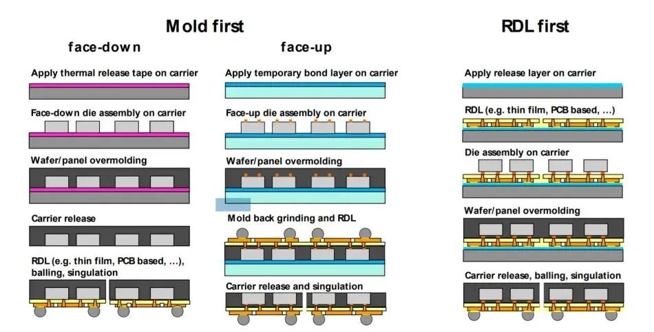
Fan-Out Wafer Level Packaging (FOWLP)
FOWLP technology is an improvement on wafer-level packaging (WLP) that provides more external connections for silicon chips. It involves embedding the chip in an epoxy moulding material and then constructing a high density redistribution layer (RDL) on the wafer surface and applying solder balls to form a reconstituted wafer.
FOWLP provides a large number of connections between the package and the application board, and because the substrate is larger than the die, the die pitch is actually more relaxed.
Example of a FOWLP package
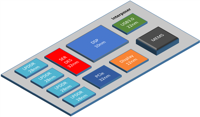
Heterogeneous integration
The integration of different components manufactured separately into higher-level assemblies can enhance functionality and improve operating characteristics, so semiconductor component manufacturers are able to combine functional components with different process flows into a single assembly.
Heterogeneous integration is similar to system-in-package (SiP), but instead of combining multiple bare dies on a single substrate, it combines multiple IPs in the form of Chiplets on a single substrate. The basic idea of heterogeneous integration is to combine multiple components with different functions in the same package.
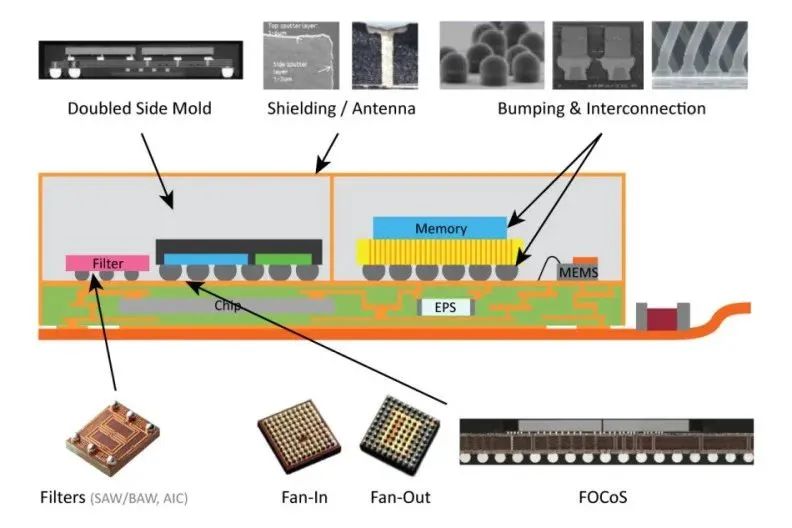
Some technical building blocks in heterogeneous integration
HBM
HBM is a standardized stack storage technology that provides high bandwidth channels for data within a stack and between memory and logical components. HBM packages stack memory die and connect them together via TSV to create more I/O and bandwidth.
HBM is a JEDEC standard that vertically integrates multiple layers of DRAM components within a package, along with application processors, GPUs and SoCs. HBM is primarily implemented as a 2.5D package for high-end servers and networking chips. The HBM2 release now addresses the capacity and clock rate limitations of the initial HBM release.
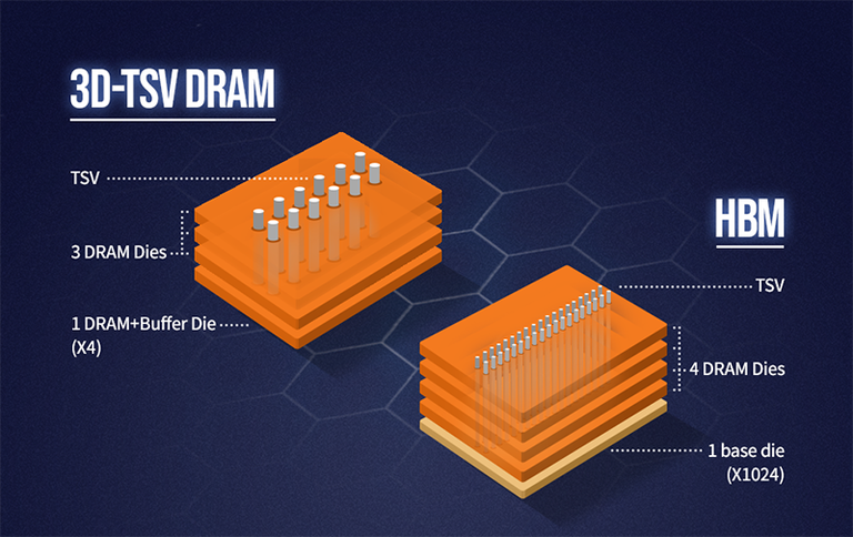
HBM packages
Intermediate Layer
The interposer layer is the conduit through which the electrical signals are passed from the multi-chip bare die or board in the package. It is the electrical interface between the sockets or connectors, allowing the signals to be propagated further away and also connected to other sockets on the board.
The interposer layer can be made of silicon and organic materials and acts as a bridge between the multi-die die and the board. Silicon interposer layers are a proven technology with high fine pitch I/O density and TSV formation capabilities and play a key role in 2.5D and 3D IC chip packaging.
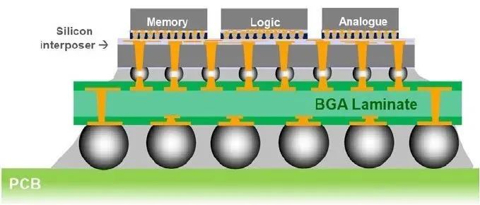
Typical implementation of a system partitioned intermediate layer
Redistribution layer
The redistribution layer contains the copper connections or alignments that enable the electrical connections between the various parts of the package. It is a layer of metallic or polymeric dielectric material that can be stacked in the package with bare die, thus reducing the I/O spacing of large chipsets. Redistribution layers have become an integral part of 2.5D and 3D package solutions, allowing the chips on them to communicate with each other using intermediary layers.
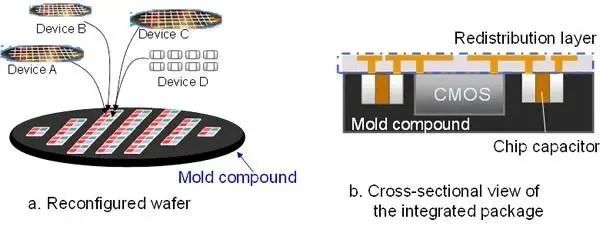
Integrated packages using redistribution layers
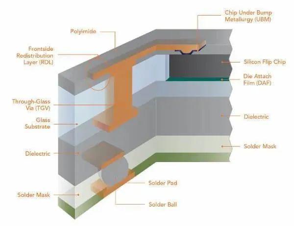
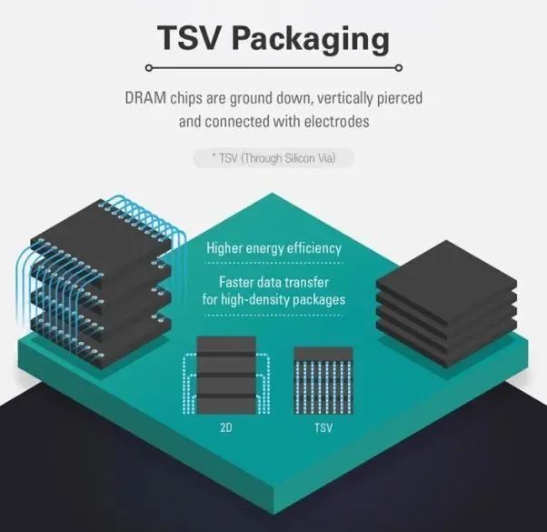
TSV
TSV is a key implementation technology for 2.5D and 3D packaging solutions and is a copper-filled wafer that provides a vertical interconnect through the silicon wafer die. It runs through the entire die to provide an electrical connection, forming the shortest path from one side of the die to the other.
Through-holes or vias are etched to a certain depth from the front side of the wafer, which is then insulated and filled by depositing a conductive material (usually copper). Once the chip is fabricated, it is thinned from the back side of the wafer to expose the vias and the metal deposited on the back side of the wafer to complete the TSV interconnect.
Post time: Jul-07-2023