
Substrate or intermediate layer is a very important part of BGA package, which can be used for impedance control and for inductor/resistor/capacitor integration in addition to interconnect wiring. Therefore, the substrate material is required to have high glass transition temperature rS (about 175~230℃), high dimensional stability and low moisture absorption, good electrical performance and high reliability. Metal film, insulation layer and substrate media should also have high adhesion properties between them.
1. The packaging process of lead bonded PBGA
① Preparation of PBGA substrate
Laminate extremely thin (12~18μm thick) copper foil on both sides of the BT resin/glass core board, then drill holes and through-hole metallization. A conventional PCB plus 3232 process is used to create graphics on both sides of the substrate, such as guide strips, electrodes, and solder area arrays for mounting solder balls. A solder mask is then added and the graphics are created to expose the electrodes and solder areas. To improve production efficiency, a substrate usually contains multiple PBG substrates.
② Packaging Process Flow
Wafer thinning → wafer cutting → chip bonding → plasma cleaning → lead bonding → plasma cleaning → molded package → assembly of solder balls → reflow oven soldering → surface marking → separation → final inspection → test hopper packaging
Chip bonding uses silver-filled epoxy adhesive to bond the IC chip to the substrate, then gold wire bonding is used to realize the connection between the chip and the substrate, followed by molded plastic encapsulation or liquid adhesive potting to protect the chip, solder lines and pads. A specially designed pick-up tool is used to place solder balls 62/36/2Sn/Pb/Ag or 63/37/Sn/Pb with a melting point of 183°C and a diameter of 30 mil (0.75mm) on the pads, and reflow soldering is performed in a conventional reflow oven, with a maximum processing temperature of no more than 230°C. The substrate is then centrifugally cleaned with CFC inorganic cleaner to remove solder and fiber particles left on the package, followed by marking, separation, final inspection, testing, and packaging for storage. The above is the packaging process of lead bonding type PBGA.
2. Packaging process of FC-CBGA
① Ceramic substrate
The substrate of FC-CBGA is multilayer ceramic substrate, which is quite difficult to make. Because the substrate has high wiring density, narrow spacing, and many through holes, as well as the requirement of coplanarity of the substrate is high. Its main process is: firstly, the multilayer ceramic sheets are co-fired at high temperature to form a multilayer ceramic metallized substrate, then the multilayer metal wiring is made on the substrate, and then plating is performed, etc. In the assembly of CBGA, the CTE mismatch between substrate and chip and PCB board is the main factor causing the failure of CBGA products. To improve this situation, in addition to the CCGA structure, another ceramic substrate, the HITCE ceramic substrate, can be used.
②Packaging process flow
Preparation of disc bumps -> disc cutting -> chip flip-flop and reflow soldering -> bottom filling of thermal grease, distribution of sealing solder -> capping -> assembly of solder balls -> reflow soldering -> marking -> separation -> final inspection -> testing -> packaging
3. The packaging process of lead bonding TBGA
① TBGA carrier tape
The carrier tape of TBGA is usually made of polyimide material.
In the production, both sides of the carrier tape are first copper coated, then nickel and gold plated, followed by punching through-hole and through-hole metallization and production of graphics. Because in this lead bonded TBGA, the encapsulated heat sink is also the encapsulated plus solid and the core cavity substrate of the tube shell, so the carrier tape is bonded to the heat sink using pressure sensitive adhesive before encapsulation.
② Encapsulation process flow
Chip thinning→chip cutting→chip bonding→cleaning→lead bonding→plasma cleaning→liquid sealant potting→assembly of solder balls→reflow soldering→surface marking→separation→final inspection→testing→packaging
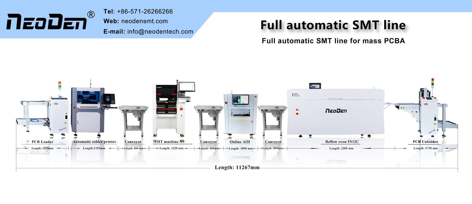
Zhejiang NeoDen Technology Co., LTD., founded in 2010, is a professional manufacturer specialized in SMT pick and place machine, reflow oven, stencil printing machine, SMT production line and other SMT Products.
We believe that great people and partners make NeoDen a great company and that our commitment to Innovation, Diversity and Sustainability ensures that SMT automation is accessible to every hobbyist on everywhere.
Add: No.18, Tianzihu Avenue, Tianzihu Town, Anji County, Huzhou City, Zhejiang Province, China
Phone: 86-571-26266266
Post time: Feb-09-2023