
Cracking of a solder joint on a plated through joint is uncommon; in Figure 1 the solder joint is on a single-sided board. The joint has failed due to expansion and contraction of the lead in the joint. In this case the fault lies with the initial design as the board is not meeting the requirements of its operating environment. Single-sided joints can fail during assembly due to poor handling but in this case the surface of the joint shows stress lines which have been produced during repeated movement.
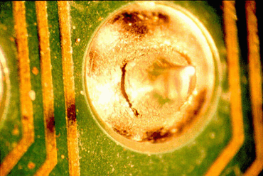
Figure 1: Stress lines here indicate that this crack on a single-sided board was caused by repeated movement during processing.
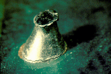
Figure 2 shows a crack around the base of the fillet and has separated from the copper pad. This is most likely to be related to the basic solderability of the board. Wetting between the solder and the pad surface has not occurred leading to joint failure. Cracking of joints would normally occur due to the thermal expansion of a joint and this would relate to the original design of the product. It is not very common for failures to occur today due to the experience and pre testing conducted by many leading electronics companies.
Figure 2: Lack of wetting between the solder and the pad surface caused this crack at the base of a fillet.
Post time: Mar-14-2020