
Most of the pcba processing factory will encounter the bad phenomenon, SMT chip components in the process of chip processing end lift. This situation has occurred in the small size chip capacitive components, especially 0402 chip capacitors, chip resistors, this phenomenon is often referred to as the “monolithic phenomenon”.
Reasons for formation
(1) components at both ends of the solder paste melting time is not synchronized or surface tension is different, such as poor printing of solder paste (one end has a defect), paste bias, components solder end size is different. Generally always solder paste after the melting end is pulled up.
(2) Pad design: pad outreach length has a suitable range, too short or too long are prone to the phenomenon of standing monument.
(3) The solder paste is brushed too thickly and the components are floated up after the solder paste has melted. In this case, the components will easily be blown by the hot air to occur the phenomenon of standing monument.
(4) Temperature curve setting: monoliths generally occur at the moment when the solder joint starts to melt. The rate of temperature rise near the melting point is very important, the slower it is the better it is to eliminate the monolith phenomenon.
(5) One of the component’s solder ends is oxidised or contaminated and cannot be wetted. Pay particular attention to components with a single layer of silver at the solder end.
(6) The pad is contaminated (with silkscreen, solder resist ink, adhered with foreign matter, oxidised).
Mechanism of formation:
When reflow soldering, the heat is applied to the top and bottom of the chip component at the same time. In general, it is always the pad with the largest exposed area that is heated first to a temperature above the melting point of the solder paste. In this way, the end of the component that is later wetted by the solder tends to be pulled up by the surface tension of the solder at the other end.
Solutions:
(1) design aspects
Reasonable design of the pad – outreach size must be reasonable, as far as possible to avoid the outreach length constitutes the outer edge of the pad (straight) wetting angle greater than 45 °.
(2) Production site
1. diligently wipe the net to ensure that the solder paste score graphics completely.
2. accurate placement position.
3. Use non-eutectic solder paste and reduce the rate of temperature rise during reflow soldering (control under 2.2℃/s).
4. Thin the thickness of the solder paste.
(3) Incoming material
Strictly control the quality of incoming material to ensure that the effective area of the components used is the same size at both ends (the basis for generating surface tension).
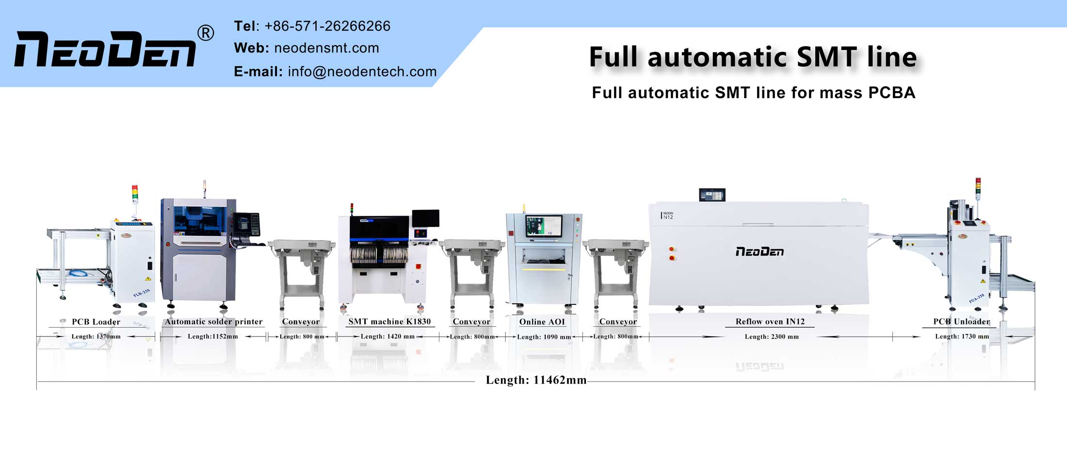
Features of NeoDen IN12C Reflow Oven
1. Built-in welding fume filtration system, effective filtration of harmful gases, beautiful appearance and environmental protection, more in line with the use of high-end environment.
2.The control system has the characteristics of high integration, timely response, low failure rate, easy maintenance, etc.
3. Intelligent, integrated with the PID control algorithm of the custom-developed intelligent control system, easy to use, powerful.
4. professional, unique 4-way board surface temperature monitoring system, so that the actual operation in a timely and comprehensive feedback data, even for complex electronic products can be effective.
5. Custom-developed stainless steel B-type mesh belt, durable and wear-resistant. Long-term use is not easy to deformation
6. Beautiful and has a red, yellow and green alarm function of the indicator design.
Post time: May-11-2023