
To meet the thermal requirements of an application, designers need to compare the thermal characteristics of different semiconductor package types. In this article, Nexperia discusses the thermal paths of its wire bond packages and chip bond packages so that designers can select a more appropriate package.
How Thermal Conduction is Achieved in Wire Bonded Devices
The primary heat sink in a wire bonded device is from the junction reference point to the solder joints on the printed circuit board (PCB), as shown in Figure 1. Following a simple algorithm of first-order approximation, the effect of the secondary power consumption channel (shown in the figure) is negligible in the thermal resistance calculation.
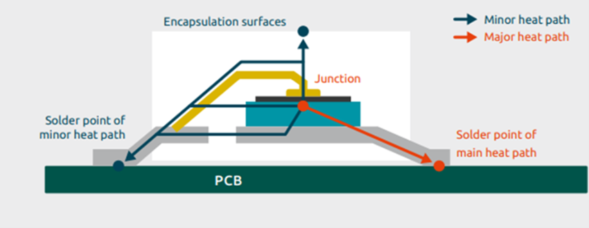
Thermal channels in wire bonded devices
Dual thermal conduction channels in a SMD device
The difference between a SMD package and a wire bonded package in terms of heat dissipation is that the heat from the junction of the device can be dissipated along two different channels, i.e., through the leadframe (as in the case of wire bonded packages) and through the clip frame.
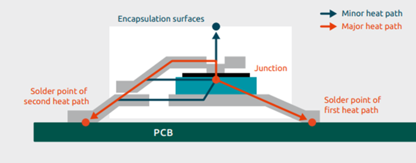
Heat transfer in a chip bonded package
The definition of the thermal resistance of the junction to the solder joint Rth (j-sp) is further complicated by the presence of two reference solder joints. These reference points may have different temperatures, causing the thermal resistance to be a parallel network.
Nexperia uses the same methodology to extract the Rth(j-sp) value for both chip-bonded and wire-soldered devices. This value characterises the main thermal path from the chip to the leadframe to the solder joints, making the values for the chip-bonded devices similar to the values for the wire-soldered devices in a similar PCB layout. However, the second channel is not fully utilised when extracting the Rth(j-sp) value, so the overall thermal potential of the device is typically higher.
In fact, the second critical heat sink channel gives designers the opportunity to improve the PCB design. For example, for a wire-soldered device, heat can only be dissipated through one channel (most of the heat of a diode is dissipated through the cathode pin); for a clip-bonded device, heat can be dissipated at both terminals.
Simulation of Thermal Performance of Semiconductor Devices
Simulation experiments have shown that thermal performance can be significantly improved if all device terminals on the PCB have thermal paths. For example, in the CFP5-packaged PMEG6030ELP diode (Figure 3), 35% of the heat is transferred to the anode pins through the copper clamps and 65% is transferred to the cathode pins through the leadframes.
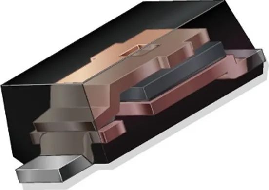
CFP5 packaged diode
“Simulation experiments have confirmed that splitting the heat sink into two parts (as shown in Figure 4) is more conducive to heat dissipation.
If a 1 cm² heatsink is split into two 0.5 cm² heatsinks placed underneath each of the two terminals, the amount of power that can be dissipated by the diode at the same temperature increases by 6%.
Two 3 cm² heatsinks increase the power dissipation by about 20 per cent compared to a standard heat sink design or a 6 cm² heatsink attached only at the cathode.”
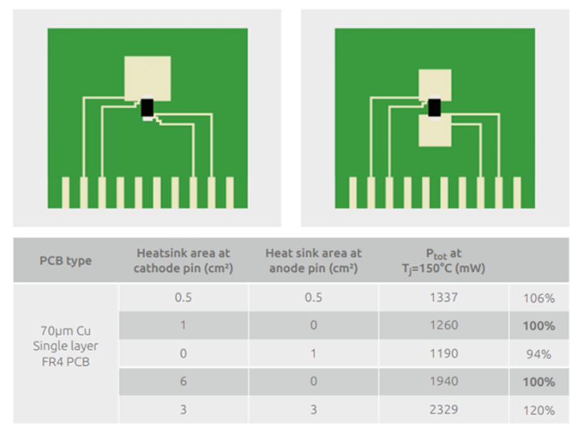
Thermal Simulation Results with Heat Sinks in Different Areas and Board Locations
Nexperia Helps Designers Select Packages Better Suited to Their Applications
Some semiconductor device manufacturers do not provide designers with the necessary information to determine which package type will provide better thermal performance for their application. In this article, Nexperia describes the thermal paths in its wire bonded and chip bonded devices to help designers make better decisions for their applications.
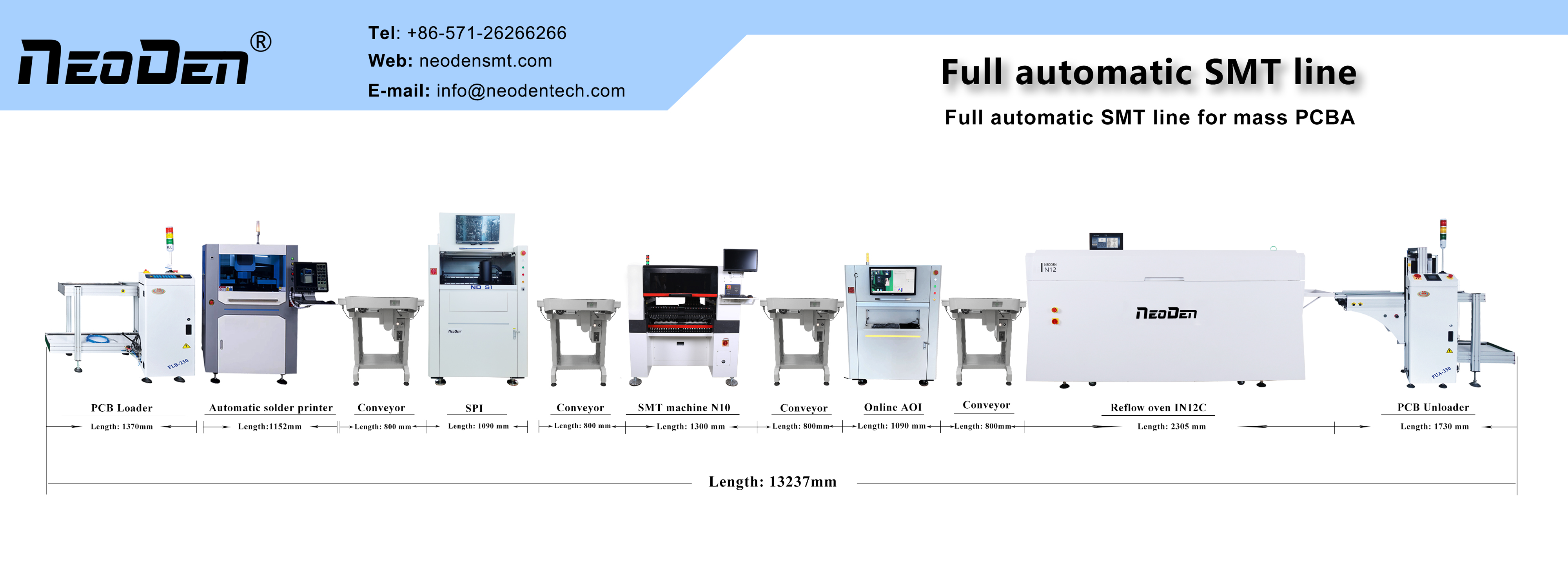
Quick facts about NeoDen
① Established in 2010, 200+ employees, 8000+ Sq.m. factory
② NeoDen products: Smart series PNP machine, NeoDen K1830, NeoDen4, NeoDen3V, NeoDen7, NeoDen6, TM220A, TM240A, TM245P, reflow oven IN6, IN12, Solder paste printer FP2636, PM3040
③ Successful 10000+ customers across the globe
④ 30+ Global Agents covered in Asia, Europe, America, Oceania and Africa
⑤ R&D Center: 3 R&D departments with 25+ professional R&D engineers
⑥ Listed with CE and got 50+ patents
⑦ 30+ quality control and technical support engineers, 15+ senior international sales, timely customer responding within 8 hours, professional solutions providing within 24 hours
Post time: Sep-13-2023