
What is Narrow Pulse Phenomenon
As a kind of power switch, IGBT needs a certain reaction time from the gate level signal to the device switching process, just as it is easy to squeeze the hand too fast in life to switch the gate, too short opening pulse may cause too high voltage spikes or high frequency oscillation problems. This phenomenon occurs helplessly from time to time as the IGBT is driven by high-frequency PWM modulated signals. The smaller the duty cycle, the easier it is to output narrow pulses, and the reverse recovery characteristics of the IGBT anti-parallel renewal diode FWD become faster during hard-switching renewal. To 1700V/1000A IGBT4 E4, the specification in the junction temperature Tvj.op = 150 ℃, the switching time tdon = 0.6us, tr = 0.12us and tdoff = 1.3us, tf = 0.59us, narrow pulse width can not be less than the sum of the specification switching time. In practice, due to the different load characteristics like photovoltaic and energy storage overwhelmingly when the power factor of + / – 1, the narrow pulse will appear near the current zero point, like reactive power generator SVG, active filter APF power factor of 0, the narrow pulse will appear near the maximum load current, the actual application of the current near the zero point is more likely to appear on the output waveform high-frequency oscillation, EMI problems ensues.
Narrow pulse phenomenon of the cause
From the semiconductor fundamentals, the main reason for the narrow pulse phenomenon is due to the IGBT or FWD just started to turn on, not immediately filled with carriers, when the carrier spread when shutting down the IGBT or diode chip, compared with the carrier completely filled after shutdown, di / dt may increase. The corresponding higher IGBT turn-off overvoltage will be generated under the commutation stray inductance, which may also cause a sudden change in diode reverse recovery current and thus snap-off phenomenon. However, this phenomenon is closely related to IGBT and FWD chip technology, device voltage and current.
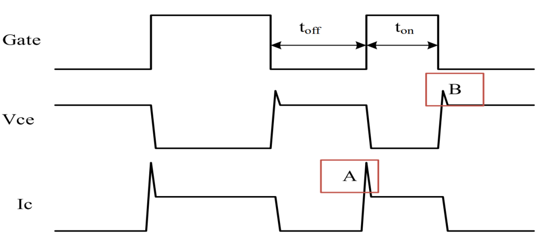
First, we have to start from the classic double pulse schematic, the following figure shows the switching logic of IGBT gate drive voltage, current and voltage. From the driving logic of IGBT, it can be divided into narrow pulse off time toff, which actually corresponds to the positive conduction time ton of diode FWD, which has a great influence on the reverse recovery peak current and recovery speed, such as point A in the figure, the maximum peak power of reverse recovery cannot exceed the limit of FWD SOA; and narrow pulse turn-on time ton, this has a relatively large impact on the IGBT turn-off process, such as point B in the figure, mainly the IGBT turn-off voltage spikes and current trailing oscillations.
But too narrow pulse device turn-on turn-off will cause what problems? In practice, what is the minimum pulse width limit that is reasonable? These problems are difficult to derive universal formulas to directly calculate with theories and formulas, theoretical analysis and research is also relatively small. From the actual test waveform and results to see the graph to speak, analysis and summary of the characteristics and commonalities of the application, more conducive to help you understand this phenomenon, and then optimize the design to avoid problems.
IGBT narrow pulse turn-on
IGBT as an active switch, using actual cases to see the graph to speak of this phenomenon is more convincing, to have some material dry goods.
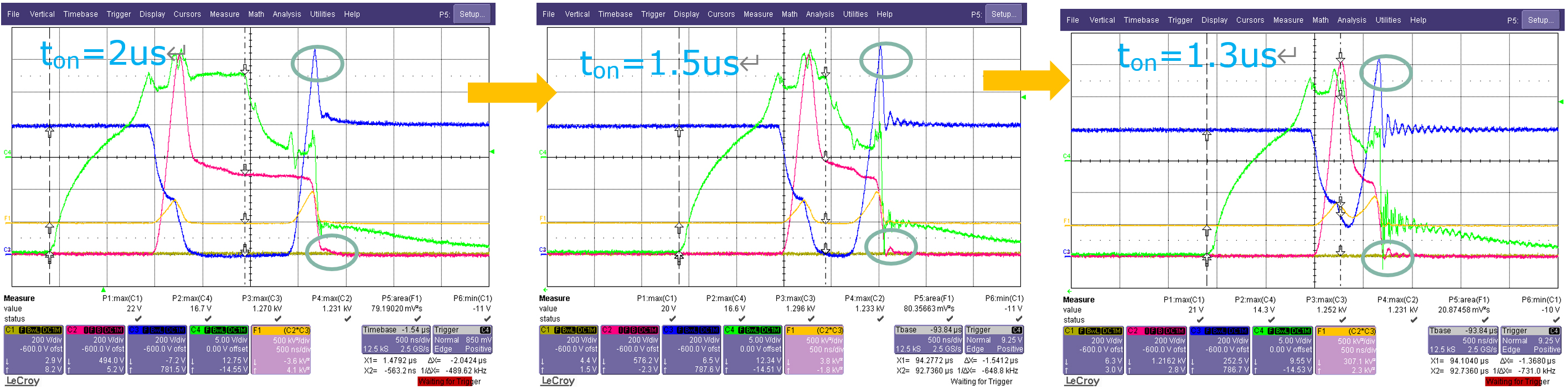
Using the high-power module IGBT4 PrimePACK™ FF1000R17IE4 as the test object, the device turn-off characteristics when the ton changes under the conditions of Vce=800V, Ic=500A, Rg=1.7Ω Vge=+/-15V, Ta=25℃, red is the collector Ic, blue is the voltage at both ends of the IGBT Vce, green is the drive voltage Vge. Vge. pulse ton decreases from 2us to 1.3us to see the change of this voltage spike Vcep, the following figure visualizes the test waveform progressively to see the change process, especially shown in the circle.
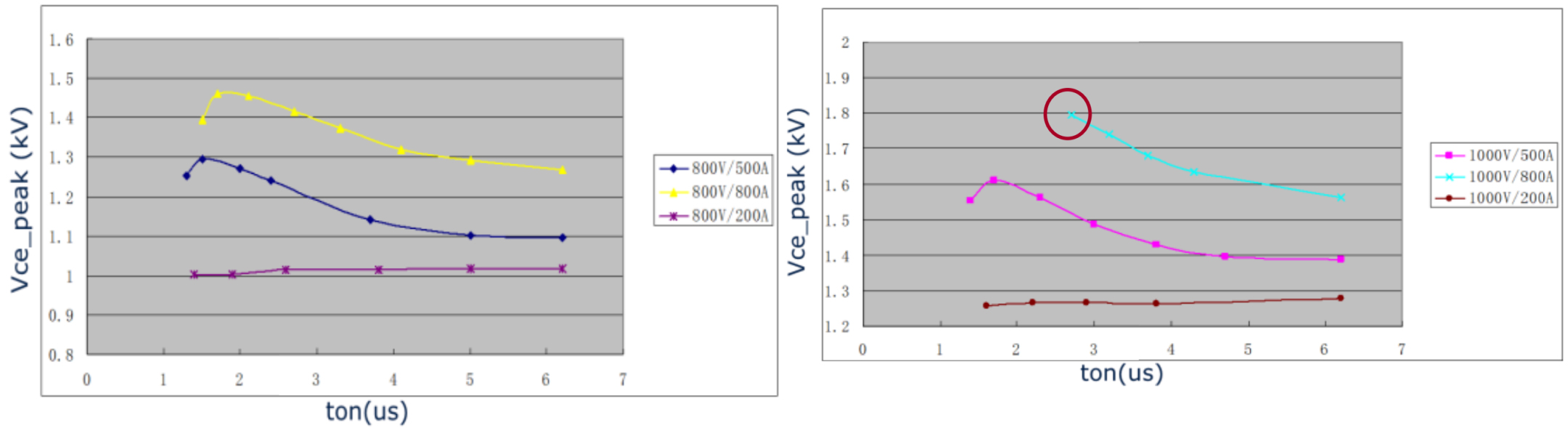
When ton changes the current Ic, in the Vce dimension to see the change in characteristics caused by ton. The left and right graphs show the voltage spikes Vce_peak at different currents Ic under the same Vce=800V and 1000V conditions respectively. from the respective test results, ton has a relatively small effect on the voltage spikes Vce_peak at small currents; when the turn-off current increases, the narrow pulse turn-off is prone to sudden changes in current and subsequently causes high voltage spikes. Taking the left and right graphs as coordinates for comparison, ton has a greater impact on the shutdown process when Vce and current Ic are higher, and is more likely to have a sudden current change. From the test to see this example FF1000R17IE4, the minimum pulse ton the most reasonable time not less than 3us.
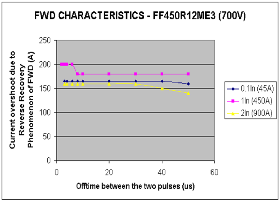
Is there a difference between the performance of high current modules and low current modules on this issue? Take FF450R12ME3 medium power module as an example, the following figure shows the voltage overshoot when the ton changes for different test currents Ic.
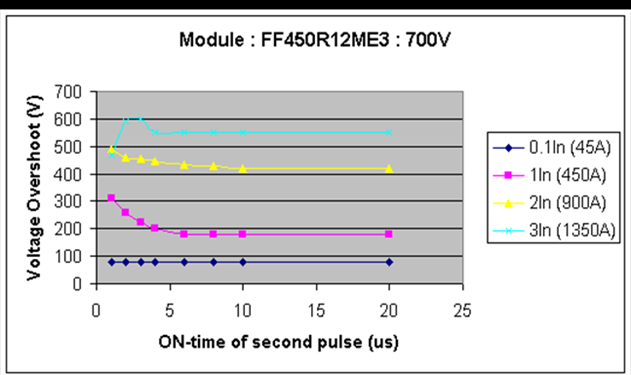
Similar results, the effect of ton on turn-off voltage overshoot is negligible at low current conditions below 1/10*Ic. When the current is increased to the rated current of 450A or even 2*Ic current of 900A, the voltage overshoot with ton width is very obvious. In order to test the performance of the characteristics of the operating conditions under extreme conditions, 3 times the rated current of 1350A, the voltage spikes have exceeded the blocking voltage, being embedded in the chip at a certain voltage level, independent of the ton width.
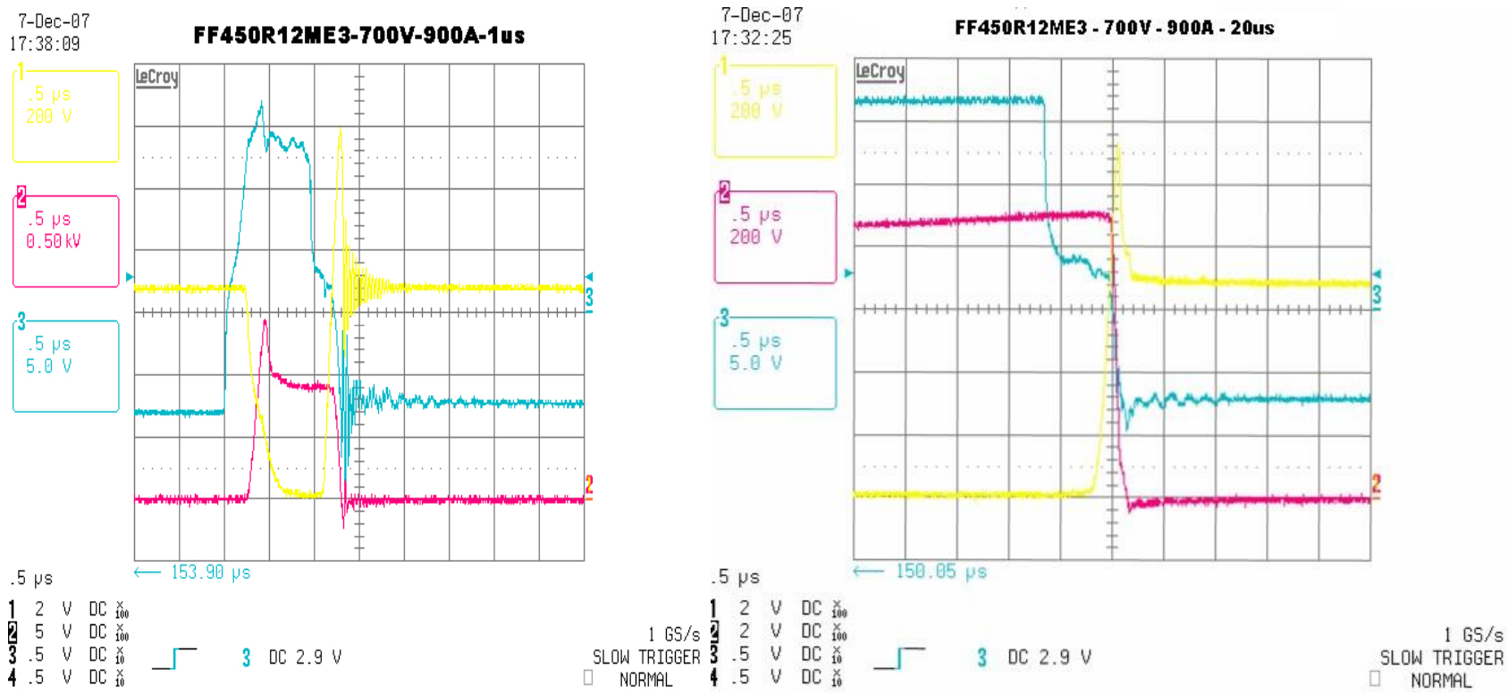
The following figure shows the comparison test waveforms of ton=1us and 20us at Vce=700V and Ic=900A. From the actual test, the module pulse width at ton=1us has started to oscillate, and the voltage spike Vcep is 80V higher than ton=20us. Therefore, it is recommended that the minimum pulse time should not be less than 1us.
FWD narrow pulse turn-on
In the half-bridge circuit, the IGBT turn-off pulse toff corresponds to the FWD turn-on time ton. The figure below shows that when the FWD turn-on time is less than 2us, the FWD reverse current peak will increase at the rated current of 450A. When toff is greater than 2us, the peak FWD reverse recovery current is basically unchanged.
IGBT5 PrimePACK™3 + FF1800R17IP5 to observe the characteristics of high-power diodes, especially under low-current conditions with ton changes, the following row shows the VR = 900V, 1200V conditions, in the small current IF = 20A conditions of the direct comparison of the two waveforms, it is clear that when ton = 3us, the oscilloscope has been unable to hold The amplitude of this high frequency oscillation. This also proves that the high-frequency oscillation of the load current over zero point in high-power device applications and the FWD short-time reverse recovery process are closely related.
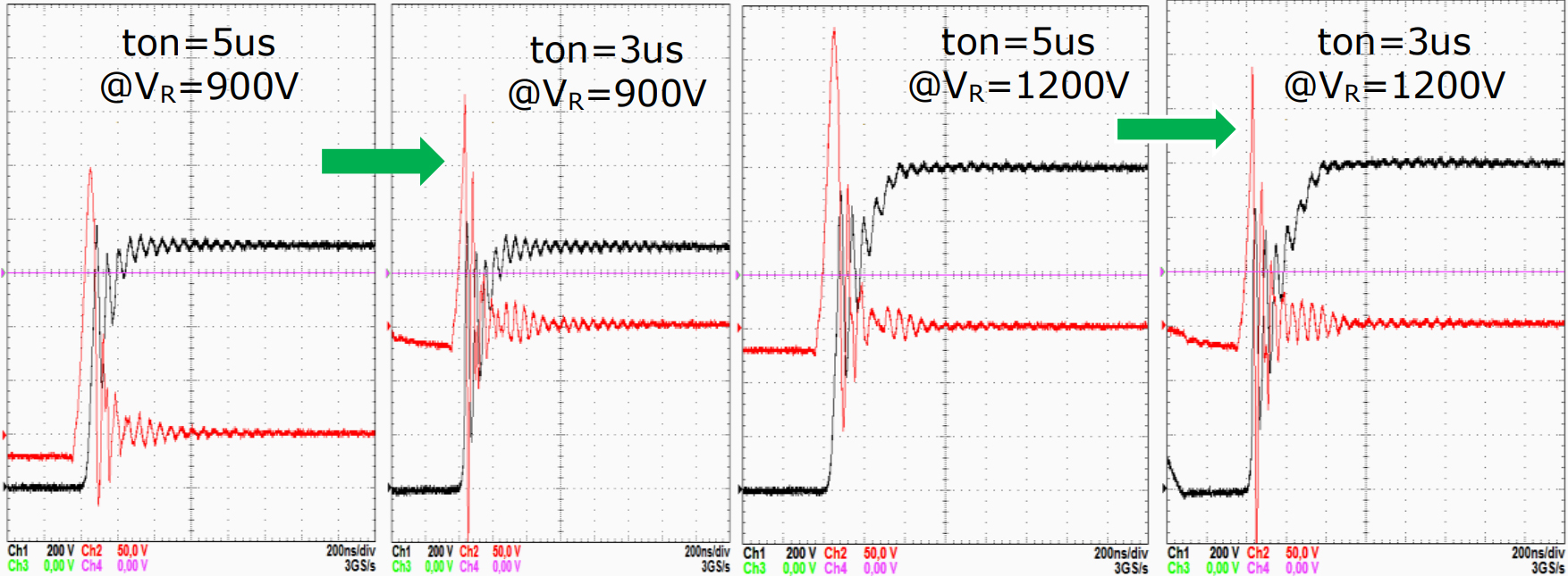
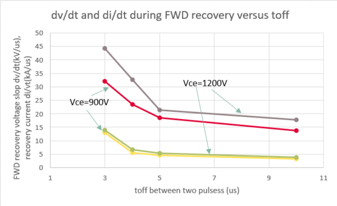
After looking at the intuitive waveform, use the actual data to further quantify and compare this process. dv/dt and di/dt of the diode vary with toff, and the smaller the FWD conduction time, the faster its reverse characteristics will become. When the higher the VR at both ends of the FWD, as the diode conduction pulse becomes narrower, its diode reverse recovery speed will be accelerated, specifically looking at the data in ton = 3us conditions.
VR = 1200V when.
dv/dt=44.3kV/us; di/dt=14kA/us.
At VR=900V.
dv/dt=32.1kV/us; di/dt=12.9kA/us.
In view of ton=3us, the waveform high-frequency oscillation is more intense, and beyond the diode safe working area, the on-time should not be less than 3us from the diode FWD point of view.
In the specification of high-voltage 3.3kV IGBT above, the FWD forward conduction time ton has been clearly defined and required, taking 2400A/3.3kV HE3 as an example, the minimum diode conduction time of 10us has been clearly given as a limit, which is mainly because the system circuit stray inductance in high-power applications is relatively large, the switching time is relatively long, and the transient in the process of device opening It is easy to exceed the maximum allowable diode power consumption PRQM.

From the actual test waveforms and results of the module, look at the graphs and talk about some basic summaries.
1. the impact of pulse width ton on IGBT turn off small current (about 1/10*Ic) is small and can actually be ignored.
2. the IGBT has a certain dependence on pulse width ton when turning off high current, the smaller the ton the higher the voltage spike V, and the turn-off current trailing will change abruptly and high frequency oscillation will occur.
3. The FWD characteristics accelerate the reverse recovery process as the on-time becomes shorter, and the shorter the FWD on-time will cause large dv/dt and di/dt, especially under low-current conditions. In addition, high-voltage IGBTs are given a clear minimum diode turn-on time tonmin=10us.
The actual test waveforms in the paper have given some reference minimum time to play a role.
Zhejiang NeoDen Technology Co., Ltd. has been manufacturing and exporting various small pick and place machines since 2010. Taking advantage of our own rich experienced R&D, well trained production, NeoDen wins great reputation from the world wide customers.
With global presence in over 130 countries, the excellent performance, high accuracy and reliability of NeoDen PNP machines make them perfect for R&D, professional prototyping and small to medium batch production. We provide professional solution of one stop SMT equipment.
Add: No.18, Tianzihu Avenue, Tianzihu Town, Anji County, Huzhou City, Zhejiang Province, China
Phone: 86-571-26266266
Post time: May-24-2022