
There are five standard technologies used in printed circuit board manufacturing.
1. Machining: This includes drilling, punching and routing holes in the printed circuit board using standard existing machinery, as well as new technologies such as laser and water jet cutting. The strength of the board needs to be considered when processing precise apertures. Small holes make this method costly and less reliable because of the reduced aspect ratio, which also makes plating difficult.
2. Imaging: This step transfers the circuit artwork to the individual layers. Single-sided or double-sided printed circuit boards can be printed using simple screen printing techniques, creating a print and etch based pattern. But this has a minimum line width limit that can be achieved. For fine circuit boards and multilayers, optical imaging techniques are used for flood screen printing, dip coating, electrophoresis, roller lamination, or liquid roller coating. In recent years, direct laser imaging technology and liquid crystal light valve imaging technology have also been widely used. 3.
3. lamination: This process is mainly used to manufacture multilayer boards, or substrates for single/dual panels. The layers of glass panels impregnated with b-grade epoxy resin are pressed together with a hydraulic press to bond the layers together. The pressing method can be cold press, hot press, vacuum assisted pressure pot, or vacuum pressure pot, providing tight control over the media and thickness. 4.
4. Plating: Basically a metallization process that can be achieved by wet chemical processes such as chemical and electrolytic plating, or by dry chemical processes such as sputtering and CVD. While chemical plating provides high aspect ratios and no external currents, thus forming the core of additive technology, electrolytic plating is the preferred method for bulk metallization. Recent developments such as electroplating processes offer higher efficiency and quality while reducing environmental taxation.
5. Etching: The process of removing unwanted metals and dielectrics from a circuit board, either dry or wet. The uniformity of etching is a primary concern at this stage, and new anisotropic etching solutions are being developed to expand the capabilities of fine line etching.
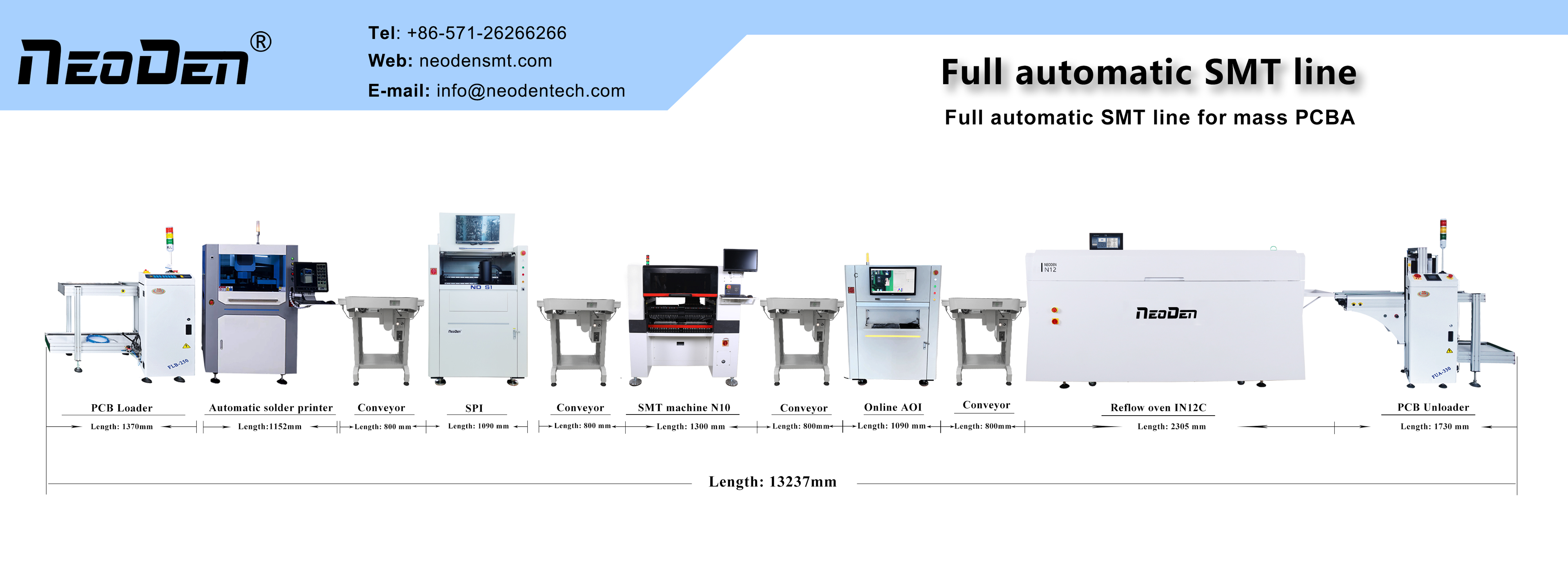
Features of NeoDen ND2 Automatic Stencil Printer
1. Accurate optical positioning system
Four way light source is adjustable, light intensity is adjustable, light is uniform, and image acquisition is more perfect.
Good identification (including uneven mark points), suitable for tinning, copper plating, Gold plating, tin spraying, FPC and other types of PCB with different colors.
2. Intelligent squeegee system
Intelligent programmable setting, two independent direct motors driven squeegee, built-in precise pressure control system.
3. High efficiency and high adaptability stencil cleaning system
The new wiping system ensures full contact with the stencil.
Three cleaning methods of dry, wet and vacuum, and free combination can be selected; soft wear-resistant rubber wiping plate, thorough cleaning, convenient disassembly, and universal length of wiping paper.
4. 2D solder paste printing quality inspection and SPC analysis
The 2D function can quickly detect the printing defects such as offset, less tin, missing printing and connecting tin, and the detection points can be increased arbitrarily.
SPC software can ensure the printing quality through the sample analysis machine CPK index collected by the machine.
Post time: Feb-10-2023