
Reverse current is when the voltage at the output of a system is higher than the voltage at the input, causing current to flow through the system in the reverse direction.
Sources:
1. the body diode becomes forward biased when the MOSFET is used for load switching applications.
2. a sudden drop in input voltage when the power supply is disconnected from the system.
Occasions where reverse current blocking needs to be considered:
1. when the power multiplexed supply is MOS controlled
2. ORing control. ORing is similar to power multiplexing, except that instead of selecting a power supply to power the system, the highest voltage is always used to power the system.
3. slow voltage drop during power loss, especially when the output capacitance is much larger than the input capacitance.
Hazards:
1. reverse current can damage internal circuitry and power supplies
2. reverse current spikes can also damage cables and connectors
3. the body diode of the MOS rises in power consumption and can even be damaged
Optimisation methods:
1. Use diodes
Diodes, especially Schottky diodes, are naturally protected against reverse current and reverse polarity, but they are costly, have high reverse leakage currents, and require heat dissipation.
2. Use back-to-back MOS
Both directions can be blocked, but occupies a large board area, high conduction impedance, high cost.
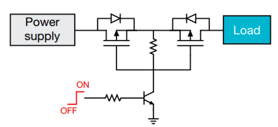
In the following figure, the control transistor conduction, its collector is low, the two PMOS conduction, when the transistor off, if the output is higher than the input, the right side of the MOS body diode conduction, so that the D level is high, making the G level is high, the left side of the MOS body diode does not pass, and at the same time, due to the MOS of the VSG for the body diode voltage drop is not up to the threshold voltage, so the two MOS shut down, which blocked the output to the input current. This blocks the current from the output to the input.
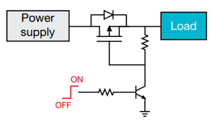
3. Reverse MOS
Reverse MOS can block the output to the input of the reverse current, but the disadvantage is that there is always a body diode path from the input to the output, and not smart enough, when the output is greater than the input, can not turn off the MOS, but also need to add a voltage comparison circuit, so there is a later ideal diode.
4. Load switch
5. Multiplexing
Multiplexing: selecting one of two or more input supplies from between them to power a single output.
6. Ideal Diode
There are two goals in forming an ideal diode, one is to simulate a Schottky and the other is that there must be an input-output comparison circuit to turn it off in reverse.
Post time: Aug-10-2023