
1) Electroforming stencil
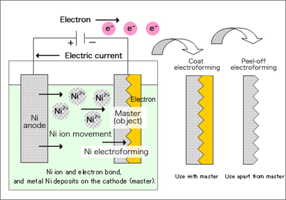
The manufacturing principle of the electroformed stencil: the electroformed template is made by printing the photoresist material on the conductive metal base plate, and then through the masking mold and ultraviolet exposure, and then the thin template is electroformed in the electroforming liquid. In fact, electroforming is similar to electroplating, except that the nickel sheet after electroforming can be stripped from the bottom plate to form a stencil.
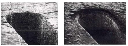
Electroforming stencil has the following characteristics: there is no stress inside the steel sheet, the hole wall is very smooth, the stencil can be any thickness (within 0.2mm, controlled by the electroforming time), the disadvantage is that the cost is high. The following figure is a comparison of the laser steel mesh and electroformed steel mesh wall. The smooth hole wall of the electroformed steel mesh has a better demoulding effect after printing, so that the opening ratio can be as low as 0.5.
2) Ladder stencil
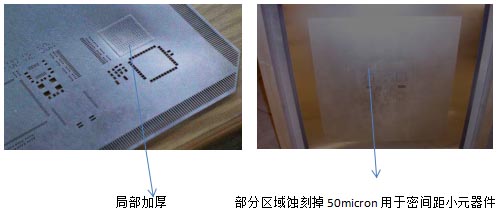
The stepped steel mesh can be locally thickened or thinned. The partially thickened part is used to print the solder pads that require a large amount of solder paste, and the thickened part is realized by electroforming, and the cost is higher. The thinning is achieved by chemical etching. The thinned part is used to print the pads of miniaturized components, which makes the demolding effect better. Users who are more cost-sensitive are recommended to use chemical etching, which is cheaper.
3) Nano Ultra Coating
Coating or plating a layer of nano-coating on the surface of the steel mesh, the nano-coating makes the hole wall repel the solder paste, so the demolding effect is better, and the volume stability of solder paste printing is more consistent. In this way, the quality of printing is more guaranteed, and the number of cleaning and wiping of the steel mesh can also be reduced. At present, most of the domestic processes only apply a layer of nano-coating, and the effect is weakened after a certain number of printing. There are nano-coatings directly plated on the steel mesh, which have better effect and durability, and of course the cost is higher.
3. Double solder paste molding process.
1) Printing/Printing
Two printing machines are used to print and form solder paste. The first one uses ordinary stencil to print the pads of small components with fine pitch, and the second one uses 3D stencil or step stencil to print the pads of large components.
This method requires two printing presses, and the cost of the stencil is also high. If a 3D stencil is used, a comb scraper is needed, which increases the cost and the production efficiency is also low.
2) Printing/spray tin
The first solder paste printer prints close-pitch small component pads, and the second inkjet printer prints large component pads. In this way, the solder paste molding effect is good, but the cost is high and the efficiency is low (depending on the number of large component pads).
Users can choose to use the above several solutions according to their own situation. In terms of cost and production efficiency, reducing the thickness of the stencil, using low-required aperture area ratio stencils, and step stencils are more suitable choices; users with low output, high quality requirements, and cost-insensitive users can choose printing/jet printing Program.
Post time: Aug-07-2020