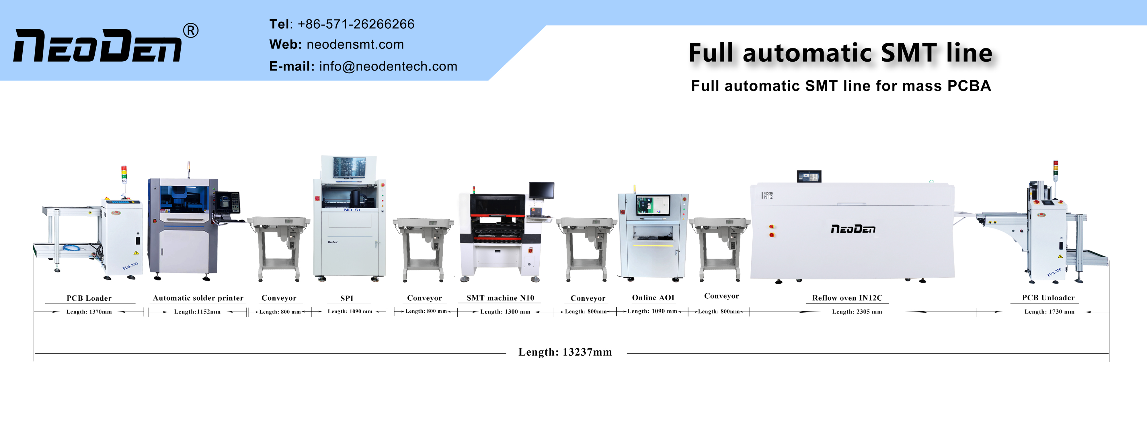
SPI inspection is an inspection process of SMD processing technology, which mainly detects the quality of solder paste printing.
SPI’s full English name is Solder Paste Inspection, its principle is similar to AOI, are through the optical acquisition and then generate pictures to determine its quality.
The working principle of SPI
In pcba mass production, engineers will print a few pcb boards, SPI inside the work camera will take pictures of the PCB (collection of printing data), after the algorithm analyzes the image generated by the work interface, and then manually visually verify whether it is ok. if ok, it will be the board’s solder paste printing data as a standard of reference for subsequent mass production will be based on the printing data to do the judgment!
Why SPI inspection
In the industry, more than 60% of the soldering defects are caused by poor solder paste printing, so adding a check after the solder paste printing than after the soldering problems and then return to the union to save costs. Because SPI inspection found bad, you can directly from the docking station to take down the bad pcb, wash off the solder paste on the pads can be reprinted, if the back of the soldering fixed and then found, then you need to use the iron repair or even scrap. Relatively speaking, you can save costs
What bad factors does SPI detect
1. Solder paste printing offset
Solder paste printing offset will cause standing monument or empty welding, because the solder paste offset one end of the pad, in the soldering heat melt, the two ends of the solder paste heat melt will appear time difference, affected by the tension, one end may be warped.
2. Solder paste printing flatness
Solder paste printing flatness indicates that the pcb pad surface solder paste is not flat, more tin at one end, less tin at one end, will also cause a short circuit or the risk of standing monument.
3. Thickness of solder paste printing
Solder paste printing thickness is too little or too much solder paste leakage printing, will cause the risk of soldering empty solder.
4. Solder paste printing whether to pull the tip
Solder paste printing pull tip and solder paste flatness is similar, because the solder paste after printing to release the mold, if too fast too slow may appear pull tip.
Specifications of NeoDen S1 SPI Machine
PCB transfer system: 900±30mm
Min PCB size: 50mm×50mm
Max PCB size: 500mm×460mm
PCB thickness: 0.6mm~6mm
Plate edge clearance: up: 3mm down: 3mm
Transfer speed: 1500mm/s (MAX)
Plate bending compensation: <2mm
Driver equipment: AC servo motor system
Setting accuracy: <1 μm
Moving speed: 600mm/s
Post time: Jul-20-2023

