
1. Choosing the Right Materials
Selecting the right materials is essential for creating high-quality induction PCBs. The choice of materials will depend on the specific requirements of the circuit and the operating frequency range. For example, FR-4 is a common material used for lower frequency PCBs. On the other hand, Rogers or PTFE materials are often good for higher frequency ranges. It is also important to choose materials with low dielectric loss and high thermal conductivity. This will minimize signal loss and heat buildup.
2. Determining Trace Widths and Spacings
Determining the appropriate trace widths and spacings is critical for achieving proper signal performance and reducing electromagnetic interference. This can be a complex process that involves calculating impedance, signal loss, and other factors that affect signal quality. PCB design software can help automate this process. However, it is important to understand the underlying principles to ensure accurate results.
3. Adding Grounded Planes
Grounded planes are essential for reducing electromagnetic interference and improving signal quality in induction PCBs. They help to shield the circuit from external electromagnetic fields. This is how it reduces crosstalk between adjacent signal traces.
4. Creating Stripline and Microstrip Transmission Lines
Stripline and microstrip transmission lines are specialized trace configurations in induction PCBs to transmit high-frequency signals. Stripline transmission lines consist of a signal trace sandwiched between two grounded planes. However, Microstrip transmission lines have signal trace on one layer and a grounded plane on the opposite layer. These trace configurations help to minimize signal loss and interference and ensure consistent signal quality across the circuit.
5. Fabricating the PCB
Once the design is complete, the designers fabricate PCB using either the subtractive or additive process. The subtractive process involves etching away unwanted copper using a chemical solution. On the contrary, the additive process involves depositing copper onto a substrate using electroplating. Both processes have their advantages and disadvantages, and the choice will depend on the specific requirements of the circuit.
6. Assembly and Testing
After the fabrication of PCBs, the designers assemble them onto the board. After this they test the circuit for functionality and performance. Testing can involve measuring signal quality, checking for shorts and opens, and verifying the operation of individual components.
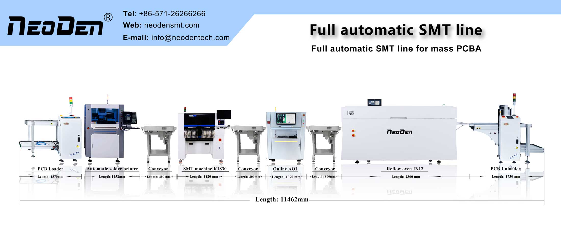
Quick facts about NeoDen
① Established in 2010, 200+ employees, 8000+ Sq.m. factory
② NeoDen products: Smart series PNP machine, NeoDen K1830, NeoDen4, NeoDen3V, NeoDen7, NeoDen6, TM220A, TM240A, TM245P, reflow oven IN6, IN12, Solder paste printer FP2636, PM3040
③ Successful 10000+ customers across the globe
④ 30+ Global Agents covered in Asia, Europe, America, Oceania and Africa
⑤ R&D Center: 3 R&D departments with 25+ professional R&D engineers
⑥ Listed with CE and got 50+ patents
⑦ 30+ quality control and technical support engineers, 15+ senior international sales, timely customer responding within 8 hours, professional solutions providing within 24 hours
Post time: Apr-11-2023