
SMT chip processing gradually to high density, fine pitch design development, the minimum spacing of components design, need to consider the SMT manufacturer’s experience and process perfection. The design of the minimum spacing of components, in addition to ensuring the safety distance between SMT pads, should also consider the maintainability of components.
Ensure safe spacing when laying out components
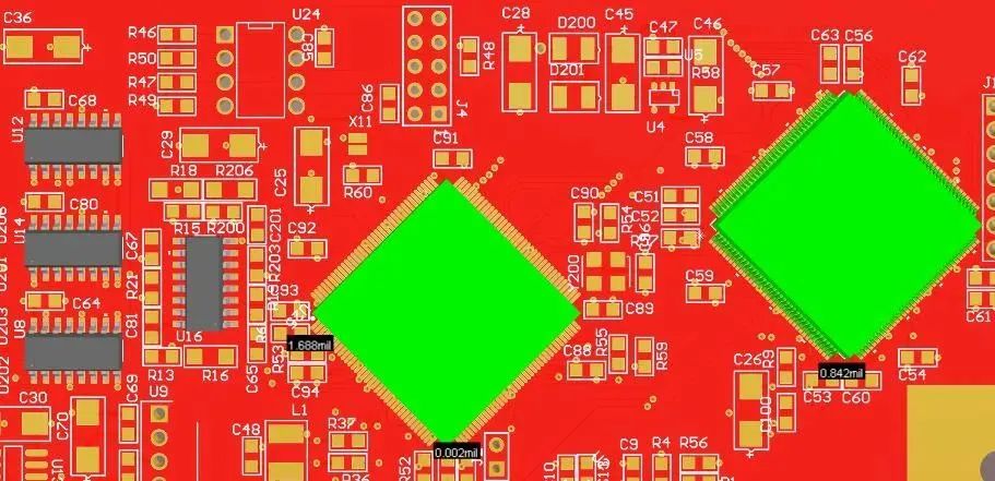
1. The safety distance is related to the stencil flare, the stencil opening is too large, the stencil thickness is too large, the stencil tension is not enough stencil deformation, there will be welding bias, resulting in components even tin short circuit.
2. In work such as hand soldering, selective soldering, tooling, rework, inspection, testing, assembly and other operating space, the distance is also required.
3. The size of the spacing between chip devices is related to the pad design, if the pad does not extend out of the component package, the solder paste will creep up along the component end of the solder side, the thinner the component the easier it is to bridge even a short circuit.
4. The safety value of the spacing between components is not an absolute value, as manufacturing equipment is not the same, there are differences in the ability to make the assembly, the safety value can be defined as severity, possibility, safety.
Defects of unreasonable component layout
Components in the PCB on the correct installation layout, is an extremely important part of the reduction of welding defects, component layout, should be as far as possible from the deflection of a large area and high stress areas, the distribution should be as uniform as possible, especially for components with a large thermal capacity, should try to avoid the use of oversized PCB to prevent warping, poor layout design will directly affect the PCBA assembleability and reliability.
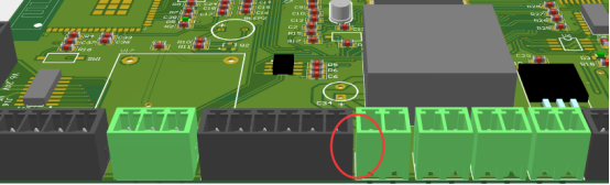
1. Connector distance is too close
Connectors are generally higher components, in the layout of time distance too close, assembled next to each other after the spacing is too small, does not have the reworkability.
2. Distance of different devices
In SMT, because of the small spacing of devices prone to bridging phenomenon, different devices bridging more than occur in 0.5mm and below the spacing, because of its small spacing, so the stencil template design or printing a slight omission is very easy to produce bridging, and the spacing of components is too small, there is a risk of short circuit.
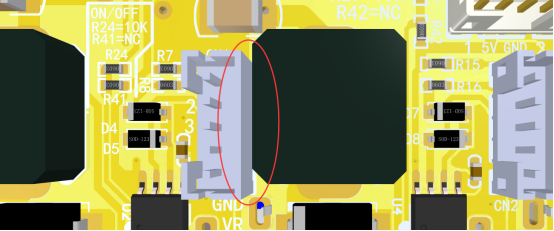
3. Assembly of two large components
The thickness of the two components closely lined up together, will cause the placement machine in the placement of the second component, touch the front has been posted components, the detection of danger caused by the machine automatically power off.
4. Small components under large components
Large components below the placement of small components, will cause the consequences of the inability to repair, for example, digital tube under the resistor, will cause difficulties to repair, repair must first remove the digital tube to repair, and may cause digital tube damage.
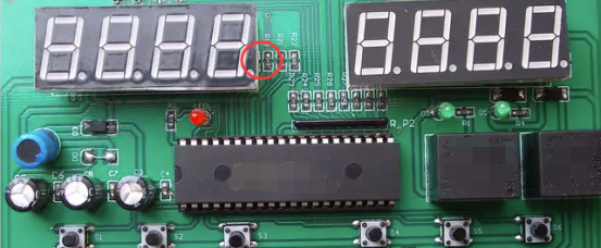
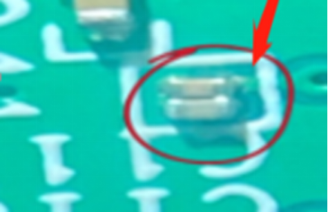
Case of short circuit caused by too close a distance between components
>> Problem Description
A product in SMT chip production, found that the capacitor C117 and C118 material distance is less than 0.25mm, SMT chip production has even tin short circuit phenomenon.
>> Problem Impact
It caused a short circuit in the product and affected the product function; to improve it, we need to change the board and increase the distance of the capacitor, which also affects the product development cycle.
>> Problem Extension
If the spacing is not particularly close, and the short circuit is not obvious, there will be a safety hazard, and the product will be used by the user with short circuit problems, causing unimaginable losses.
Post time: Apr-18-2023