
LED driver chip introduction
with the rapid development of the automotive electronics industry, high-density LED driver chips with wide input voltage range are widely used in automotive lighting, including exterior front and rear lighting, interior lighting and display backlighting.
LED driver chips can be divided into analog dimming and PWM dimming according to the dimming method. Analog dimming is relatively simple, PWM dimming is relatively complex, but the linear dimming range is greater than analog dimming. LED driver chip as a class of power management chip, its topology mainly Buck and Boost. buck circuit output current continuous so that its output current ripple is smaller, requiring smaller output capacitance, more conducive to achieve high power density of the circuit.
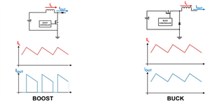 Figure 1 Output Current Boost vs Buck
The common control modes of LED driver chips are current mode (CM), COFT (controlled OFF-time) mode, COFT & PCM (peak current mode) mode. Compared to the current mode control, COFT control mode does not require loop compensation, which is conducive to improving power density, while having a faster dynamic response.
Unlike other control modes, the COFT control mode chip has a separate COFF pin for off-time setting. This article introduces the configuration and precautions for the external circuit of COFF based on a typical COFT-controlled Buck LED driver chip.
Basic configuration of COFF and precautions
The control principle of COFT mode is that when the inductor current reaches the set off current level, the upper tube turns off and the lower tube turns on. When the turn-off time reaches tOFF, the upper tube turns on again. After the upper tube turns off, it will remain off for a constant time (tOFF). tOFF is set by the capacitor (COFF) and output voltage (Vo) at the periphery of the circuit. This is shown in Figure 2. Because the ILED is tightly regulated, Vo will remain nearly constant over a wide range of input voltages and temperatures, resulting in a nearly constant tOFF, which can be calculated using Vo.
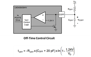 Figure 2. off time control circuit and tOFF calculation formula
It should be noted that when the selected dimming method or dimming circuit requires a shorted output, the circuit will not start properly at this time. At this time, the inductor current ripple becomes large, the output voltage becomes very low, far less than the set voltage. When this failure occurs, the inductor current will work with the maximum off time. Usually the maximum off time set inside the chip reaches 200us~300us. At this time the inductor current and output voltage seem to enter a hiccup mode and cannot output normally. Figure 3 shows the abnormal waveform of the inductor current and output voltage of the TPS92515-Q1 when the shunt resistor is used for the load.
Figure 4 shows three types of circuits that may cause the above faults. When the shunt FET is used for dimming, the shunt resistor is selected for the load, and the load is an LED switching matrix circuit, all of them may short out the output voltage and prevent normal start-up.
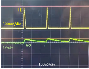 Figure 3 TPS92515-Q1 Inductor Current and Output Voltage (Resistor Load Output Short Fault)
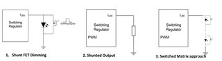
Figure 4. Circuits that may cause output shorts
To avoid this, even when the output is shorted, an additional voltage is still needed to charge the COFF. The parallel supply that VCC/VDD can be used as charges the COFF capacitors, maintains a stable off time, and keeps a constant ripple. Customers can reserve a resistor ROFF2 between VCC/VDD and COFF when designing the circuit, as shown in Figure 5, to facilitate the debugging work later. At the same time, the TI chip datasheet usually gives the specific ROFF2 calculation formula according to the internal circuit of the chip to facilitate the customer’s choice of resistor.
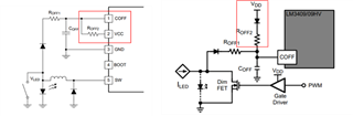 Figure 5. SHUNT FET External ROFF2 Improvement Circuit
Taking the short-circuit output fault of TPS92515-Q1 in Figure 3 as an example, the modified method in Figure 5 is used to add a ROFF2 between VCC and COFF to charge the COFF.
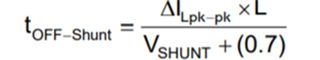
Selecting ROFF2 is a two-step process. The first step is to calculate the required shutdown time (tOFF-Shunt) when the shunt resistor is used for the output, where VSHUNT is the output voltage when the shunt resistor is used for the load.
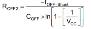 The second step is to use tOFF-Shunt to calculate ROFF2, which is the charge from VCC to COFF via ROFF2, calculated as follows.
Based on the calculation, select the appropriate ROFF2 value (50k Ohm) and connect ROFF2 between VCC and COFF in the fault case in Figure 3, when the circuit output is normal. Also note that ROFF2 should be much larger than ROFF1; if it is too low, the TPS92515-Q1 will experience minimum turn-on time problems, which will result in increased current and possible damage to the chip device.
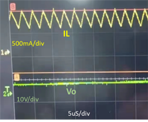 Figure 6. TPS92515-Q1 inductor current and output voltage (normal after adding ROFF2)
Post time: Feb-15-2022