
I. Pay attention to the size of the inrush current designed in the PCB wiring
In the test, often encounter the original design of the PCB can not meet the needs of the surge. General engineers design, only take into account the functional design of the system, such as the actual work of the system only needs to carry 1A of current, the design will be designed according to this, but it is possible that the system needs to be designed for surge, transient surge current to reach 3KA (1.2/50us & 8/20us), so now I go by 1A of the actual working current design, whether it can achieve the above transient surge capacity? The actual experience of the project is to tell us that this is impossible, so how to do well? Here is a way to calculate the PCB wiring can be used as a basis for carrying instantaneous current.
For example: 0.36mm width of 1oz copper foil, thickness 35um lines in a 40us rectangular current surge, the maximum inrush current of about 580A. If you want to do a 5KA (8/20us) protection design, then the front of the PCB wiring should be reasonable 2 oz copper foil 0.9mm width. Safety devices can be appropriate to relax the width.
II. Pay attention to the surge port components layout should be safe spacing
Surge port design in addition to our normal operating voltage design safety spacing, we must also consider the safety spacing of transient surges.
On the normal operating voltage design when the safety spacing we can refer to the relevant specifications of UL60950. In addition, we take UL in UL796 standard in the printed circuit board withstand voltage test standard is 40V / mil or 1.6KV / mm. This data guidance between the PCB conductors can withstand Hipot’s withstand voltage test safety spacing is very useful.
For example, according to 60950-1 Table 5B, 500V working voltage between the conductors should be to meet the 1740Vrms withstand voltage test, and 1740Vrms peak should be 1740X1.414 = 2460V. According to the 40V/mil setting standard, you can calculate the spacing between the two PCB conductors should not be less than 2460/40 = 62mil or 1.6mm.
And surges in addition to the above normal things to note, but also pay attention to the size of the applied surge, and the characteristics of the protection device to increase the safety spacing to 1.6mm spacing, the maximum cut-off creepage voltage of 2460V, if we surge voltage up to 6KV, or even 12KV, then whether this safety spacing to increase depends on the characteristics of the surge overvoltage protection device, which is also our Engineers often encounter in the experiment when the surge creeps loudly.
Ceramic discharge tube, for example, in the requirement of 1740V withstand voltage, we choose the device should be 2200V, and it is in the case of the above surge, its discharge spike voltage up to 4500V, at this time, according to the above calculation, our safety spacing is: 4500/1600 * 1mm = 2.8125mm.
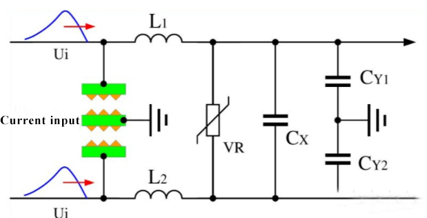
III. Pay attention to the location of overvoltage protection devices in the PCB
The location of the protective device is mainly set in the front position of the protected port, especially when the port has more than one branch or circuit, if set bypass or backward position, its protective effect performance will be greatly reduced. In reality, we sometimes because the location is not enough, or for the aesthetics of the layout, these issues are often forgotten.
IV. Pay attention to the large current return path
Large current return path must be close to the power supply or the shell of the earth, the longer the path, the greater the return impedance, the greater the magnitude of the transient current caused by the ground level rise, the impact of this voltage on many chips is great, but also the real culprit of the system reset, lockout.
Post time: Jul-14-2022