
Key points of this article
- BGA packages are compact in size and have high pin density.
- In BGA packages, signal crosstalk due to ball alignment and misalignment is called BGA crosstalk.
- BGA crosstalk depends on the location of the intruder signal and the victim signal in the ball grid array.
In multi-gate and pin-count ICs, the level of integration increases exponentially. These chips have become more reliable, robust, and easy to use thanks to the development of ball grid array (BGA) packages, which are smaller in size and thickness and larger in number of pins. However, BGA crosstalk severely affects signal integrity, thus limiting the use of BGA packages. Let’s discuss BGA packaging and BGA crosstalk.
Ball Grid Array Packages
A BGA package is a surface mount package that uses tiny metal conductor balls to mount the integrated circuit. These metal balls form a grid or matrix pattern that is arranged under the surface of the chip and connected to the printed circuit board.
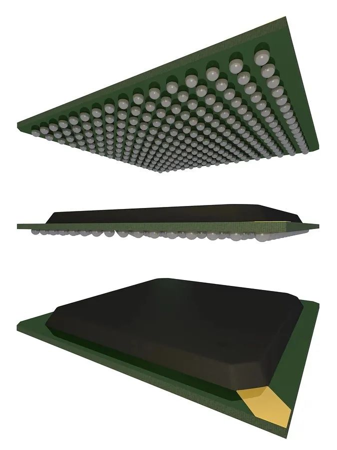
A ball grid array (BGA) package
Devices that are packaged in BGAs have no pins or leads on the periphery of the chip. Instead, the ball grid array is placed on the bottom of the chip. These ball grid arrays are called solder balls and act as connectors for the BGA package.
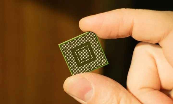
Microprocessors, WiFi chips, and FPGAs often use BGA packages. In a BGA package chip, the solder balls allow current to flow between the PCB and the package. These solder balls are physically connected to the semiconductor substrate of the electronics. Lead bonding or flip-chip is used to establish the electrical connection to the substrate and die. Conductive alignments are located within the substrate allowing electrical signals to be transmitted from the junction between the chip and the substrate to the junction between the substrate and the ball grid array.
The BGA package distributes the connection leads under the die in a matrix pattern. This arrangement provides a larger number of leads in a BGA package than in flat and double-row packages. In a leaded package, the pins are arranged at the boundaries. each pin of the BGA package carries a solder ball, which is located on the lower surface of the chip. This arrangement on the lower surface provides more area, resulting in more pins, less blocking, and fewer lead shorts. In a BGA package, the solder balls are aligned furthest apart than in a package with leads.
Advantages of BGA packages
The BGA package has compact dimensions and high pin density. the BGA package has low inductance, allowing the use of lower voltages. The ball grid array is well spaced, making it easier to align the BGA chip with the PCB.
Some other advantages of the BGA package are:
- Good heat dissipation due to the low thermal resistance of the package.
- The lead length in BGA packages is shorter than in packages with leads. The high number of leads combined with the smaller size makes the BGA package more conductive, thus improving performance.
- BGA packages offer higher performance at high speeds compared to flat packages and double in-line packages.
- The speed and yield of PCB manufacturing increases when using BGA-packaged devices. The soldering process becomes easier and more convenient, and BGA packages can be easily reworked.
BGA Crosstalk
BGA packages do have some drawbacks: solder balls cannot be bent, inspection is difficult due to the high density of the package, and high volume production requires the use of expensive soldering equipment.
To reduce BGA crosstalk, a low-crosstalk BGA arrangement is critical.
BGA packages are often used in a large number of I/O devices. Signals transmitted and received by an integrated chip in a BGA package can be disturbed by signal energy coupling from one lead to another. Signal crosstalk caused by the alignment and misalignment of solder balls in a BGA package is called BGA crosstalk. The finite inductance between the ball grid arrays is one of the causes of crosstalk effects in BGA packages. When high I/O current transients (intrusion signals) occur in the BGA package leads, the finite inductance between the ball grid arrays corresponding to the signal and return pins creates voltage interference on the chip substrate. This voltage interference causes a signal glitch that is transmitted out of the BGA package as noise, resulting in a crosstalk effect.
In applications such as networking systems with thick PCBs that use through-holes, BGA crosstalk can be common if no measures are taken to shield the through-holes. In such circuits, the long via holes placed under the BGA can cause significant coupling and generate noticeable crosstalk interference.
BGA crosstalk depends on the location of the intruder signal and the victim signal in the ball grid array. To reduce BGA crosstalk, a low-crosstalk BGA package arrangement is critical. With Cadence Allegro Package Designer Plus software, designers can optimize complex single-die and multi-die wirebond and flip-chip designs; radial, full-angle push-squeeze routing to address the unique routing challenges of BGA/LGA substrate designs. and specific DRC/DFA checks for more accurate and efficient routing. Specific DRC/DFM/DFA checks ensure successful BGA/LGA designs in a single pass. detailed interconnect extraction, 3D package modeling, and signal integrity and thermal analysis with power supply implications are also provided.
Post time: Mar-28-2023