
I. What is HDI board?
HDI board (High Density Interconnector), that is, high-density interconnect board, is the use of micro-blind buried hole technology, a circuit board with a relatively high density of line distribution. HDI board has an inner line and outer line, and then the use of drilling, hole metallization and other processes, so that each layer of the line internal connection.
II. the difference between HDI board and ordinary PCB
HDI board is generally manufactured using the accumulation method, the more layers, the higher the technical grade of the board. Ordinary HDI board is basically 1 time laminated, high-grade HDI using 2 or more times the lamination technology, while the use of stacked holes, plating filling holes, laser direct punching and other advanced PCB technology. When the density of the PCB increases beyond the eight-layer board, the cost of manufacturing with HDI will be lower than the traditional complex press-fit process.
The electrical performance and signal correctness of HDI boards are higher than traditional PCBs. In addition, HDI boards have better improvements for RFI, EMI, static discharge, thermal conductivity, etc. High Density Integration (HDI) technology can make the end product design more miniaturized, while meeting the higher standards of electronic performance and efficiency.
III. the HDI board materials
HDI PCB materials put forward some new requirements, including better dimensional stability, anti-static mobility and non-adhesive. typical materials for HDI PCB is RCC (resin-coated copper). there are three types of RCC, namely polyimide metalized film, pure polyimide film, and cast polyimide film.
The advantages of RCC include: small thickness, light weight, flexibility and flammability, compatibility characteristics impedance and excellent dimensional stability. In the process of HDI multilayer PCB, instead of the traditional bonding sheet and copper foil as an insulating medium and conductive layer, RCC can be suppressed by conventional suppression techniques with chips. non-mechanical drilling methods such as laser are then used in order to form micro-through-hole interconnections.
RCC drives the occurrence and development of PCB products from SMT (Surface Mount Technology) to CSP (Chip Level Packaging), from mechanical drilling to laser drilling, and promotes the development and advancement of PCB microvia, all of which become the leading HDI PCB material for RCC.
In the actual PCB in the manufacturing process, for the choice of RCC, there are usually FR-4 standard Tg 140C, FR-4 high Tg 170C and FR-4 and Rogers combination laminate, which are mostly used nowadays. With the development of HDI technology, HDI PCB materials must meet more requirements, so the main trends of HDI PCB materials should be
1. The development and application of flexible materials using no adhesives
2. Small dielectric layer thickness and small deviation
3 . the development of LPIC
4. Smaller and smaller dielectric constants
5. Smaller and smaller dielectric losses
6. High solder stability
7. Strictly compatible with CTE (coefficient of thermal expansion)
IV. the application of HDI board manufacturing technology
The difficulty of HDI PCB manufacturing is micro through manufacturing, through metallization and fine lines.
1. Micro-through-hole manufacturing
Micro-through-hole manufacturing has been the core problem of HDI PCB manufacturing. There are two main drilling methods.
a. For common through-hole drilling, mechanical drilling is always the best choice for its high efficiency and low cost. With the development of mechanical machining capability, its application in micro-through-hole is also evolving.
b. There are two types of laser drilling: photothermal ablation and photochemical ablation. The former refers to the process of heating the operating material to melt it and evaporate it through the through-hole formed after high energy absorption of the laser. The latter refers to the result of high-energy photons in the UV region and laser lengths exceeding 400 nm.
There are three types of laser systems used for flexible and rigid panels, namely excimer laser, UV laser drilling, and CO 2 laser. Laser technology is not only suitable for drilling, but also for cutting and forming. Even some manufacturers manufacture HDI by laser, and although laser drilling equipment is costly, they offer higher precision, stable processes and proven technology. The advantages of laser technology make it the most commonly used method in blind/buried through-hole manufacturing. Today, 99% of the HDI microvia holes are obtained by laser drilling.
2. Through metallization
The biggest difficulty in through-hole metallization is the difficulty in achieving uniform plating. For deep hole plating technology of micro-through holes, in addition to using plating solution with high dispersion ability, the plating solution on the plating device should be upgraded in time, which can be done by strong mechanical stirring or vibration, ultrasonic stirring, and horizontal spraying. In addition, the humidity of the through-hole wall must be increased before plating.
In addition to process improvements, HDI through-hole metallization methods have seen improvements in major technologies: chemical plating additive technology, direct plating technology, etc.
3. Fine Line
The implementation of fine lines includes conventional image transfer and direct laser imaging. Conventional image transfer is the same process as ordinary chemical etching to form lines.
For laser direct imaging, no photographic film is required, and the image is formed directly on the photosensitive film by laser. UV wave light is used for operation, enabling liquid preservative solutions to meet the requirements of high resolution and simple operation. No photographic film is required to avoid undesirable effects due to film defects, allowing direct connection to CAD/CAM and shortening the manufacturing cycle, making it suitable for limited and multiple production runs.
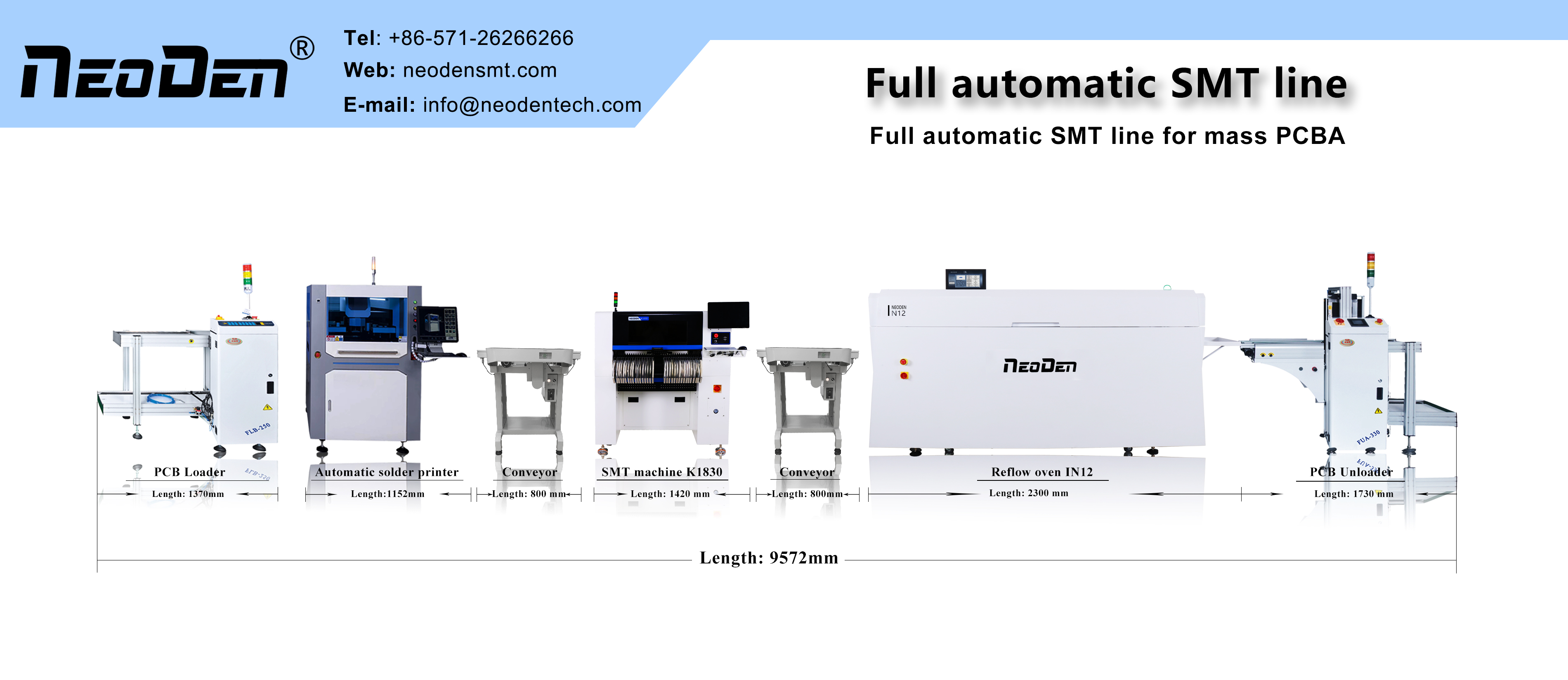
Zhejiang NeoDen Technology Co., LTD., founded in 2010, is a professional manufacturer specialized in SMT pick and place machine, reflow oven, stencil printing machine, SMT production line and other SMT Products. We have our own R & D team and own factory, taking advantage of our own rich experienced R&D, well trained production, won great reputation from the world wide customers.
In this decade, we independently developed NeoDen4, NeoDen IN6, NeoDen K1830, NeoDen FP2636 and other SMT products, which sold well all over the world.
We believe that great people and partners make NeoDen a great company and that our commitment to Innovation, Diversity and Sustainability ensures that SMT automation is accessible to every hobbyist on everywhere.
Post time: Apr-21-2022