Your Professional PCB X Ray Machine Supplier
NeoDen Tech is a global leader in manufacturing comprehensive SMT equipment. Operating from our 27,000+ m² NeoDen Park, we have evolved beyond standalone machines to become a provider of full-scale turnkey assembly lines.Our extensive product portfolio covers every critical stage of the PCBA production process. Products distributed to 130+ countries, serving applications from research laboratories to SME production lines..
Why Choose Us
Advanced Equipment
NeoDen offers a full range of SMT equipment covering the entire PCB assembly process, including high-speed pick-and-place machines, reflow ovens, stencil printers, as well as automated inspection and rework systems.
Professional Team
Backed by three specialized R&D departments and a team of 25 engineers, NeoDen holds independent intellectual property rights for its core technologies. We continuously innovate to ensure the precision and production stability of our equipment, empowering buyers with reliable, long-term automated manufacturing capabilities.
Quality Control
NeoDen strictly adheres to ISO standards, subjecting every piece of equipment—from individual components to the complete machine—to comprehensive testing. Ensuring smooth production line operations and consistent product quality control.
24H Online Service
Our offering services such as sample testing, online training, remote troubleshooting, and on-site support. Buyers are guaranteed a response within 8 hours and a resolution within 24 hours, thereby minimizing production risks.
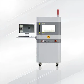
Overview of PCB X Ray Machine
A PCB X-ray machine (or Automated X-ray Inspection - AXI) is a non-destructive, high-resolution imaging system used to inspect printed circuit boards for hidden manufacturing defects. It detects faults invisible to optical systems, such as internal voids, BGA solder bridges, shorts, and component misalignment, ensuring high-quality solder joints and structural integrity in electronics manufacturing.
Product Specification
We offers the following product specifications:
|
X-Ray Tube Source |
Type: Sealed Micro-Focus X-Ray Tube |
|
Voltage Range: 40 KV - 90 KV |
|
|
Current Range: 10 μm - 200 μm |
|
|
Max Output Power: 8 W |
|
|
Micro Focus Spot Size: 15 μm |
|
|
Flat Panel Detector |
Type: TFT Industrial Dynamic FPD |
|
Pixel Matrix: 768 * 768 ~ 1536 * 1536 |
|
|
Field of View: 65 * 65 mm ~ 130 * 130 mm |
|
|
Resolution: 5.8 Lp/mm |
|
|
Frame Rate: 20 ~ 40 fps |
|
|
A/D Conversion Bit: 16 bits |
|
|
General Specifications |
Model: NeoDen ND56X |
|
Dimensions: 850 * 1000 * 1700 mm |
|
|
Max Sample Size: 280 * 320 mm |
|
|
Input Power: 220V 10A/110V 15A 50-60Hz |
|
|
Net Weight: Approx. 750KG |
Product features
High-Resolution Design: Delivers the clearest, highest-quality inspection images in minimal time.
High Frame Rate Detector: Incorporates a TFT industrial dynamic flat panel detector (FPD) with 5.8 Lp/mm resolution and frame rates up to 40 fps (1x1 mode).
16-bit A/D Conversion: Delivers high dynamic range, ensuring rich and accurate image detail.
CNC Automatic Inspection Mode: Supports rapid automatic inspection of multi-point arrays. Users can set multi-point coordinates based on product features for automated detection.
Customizable Image Algorithms: Software algorithms can be customized based on product characteristics and requirements to achieve fully automated defect detection (e.g., Y/N cracks, misalignment, dimensions).
User-Friendly Operation: Simple software operation with low operational costs.
Multi-functional measurement tools: Includes built-in measurement tools for distance, angle, radius, center distance, circumference, etc., with text annotation capability.

Inspection of defects in IC encapsulation, e.g., layer separation, cracks, voids/voids and line integrity.
Chip size measurement, line curvature measurement, component solder area proportion measurement.
Possible defects in PCB manufacturing processes, e.g., misalignment, solder bridge and opening.
Inspection and measurement of SMT solder shorts, cold solder, offset components, solder deficiency, vacuum in solder.
Inspection of defects in open, short or abnormal connections that may occur in wiring harnesses and automotive connectors.
Inspection for internal breakage or voiding in plastic or metal.
Checks for uniformity of battery stacking and electrode welding.
Inspection of seed, biological material, etc.
All of our machines will be fully checked by our quality control department before the shipment. We guarantee all of our machines have a one-year warranty (quick-wear parts not included).
Training details: Operation principles, system, and structure, safety and maintenance, software processing technique, etc.
Numerous feedback from our clients have proven that our machines are stable in performance with rare malfunction. However, we would like to handle it as follows once malfunction occurs:
- We guarantee that we will give you a clear reply within 24 hours.
- Customer service staff will assist you in analyzing the malfunction to locate the cause.
- If the malfunction is caused by improper operation of software and other soft faults, we will help solve the problem online.
- We will offer plenty of online support, like detailed technical and installation instructions via email, video, and telephone.

Package & Delivery
| Package: | Standard export package or Custom |
| Delivery: | By air express, by sea |

FAQ
As one of the leading PCB x ray machine manufacturers and suppliers in China, we offer a wide range of products with superior quality. Please feel free to buy high-grade PCB x ray machine at competitive price from our factory. Thank you for your interest in our products.
x ray inspection machine, x ray inspection equipment, pcb x ray inspection equipment