


Introduction
In PCBA manufacturing, visual inspection, automated optical inspection (AOI), and 3D X-ray inspection can detect the vast majority of defects related to geometric dimensions, bridging, or open circuits. However, quality issues hidden beneath the physical surface-such as brittle fractures within solder joints, the growth of intermetallic compounds (IMCs), and microscopic deep cracks-must be identified using destructive testing methods: microsection analysis.
Microsection Preparation Process and Standard Procedures
A prerequisite for microscopic analysis is the preparation of sections that are free of deformation and scratches and that accurately reflect the original morphology of the solder joints. The electronics laboratory must strictly adhere to the standard for sample preparation. Technicians first use a precision cutting machine to cut out the area of the PCBA containing specific BGA or QFN devices without damaging the physical structure of the target solder joints. The sample is then placed in a mold, and epoxy resin and hardener are injected for vacuum embedding, removing air bubbles to ensure the resin perfectly encapsulates the solder joint. After curing, the sample is sequentially ground using silicon carbide sandpaper with grits ranging from 180 to 2000. During the grinding process, a constant water flow must be maintained for cooling to prevent friction-generated heat from causing a secondary phase transformation in the internal metal structure of the solder joints. Finally, mechanical polishing is performed using a 0.3-micron aluminum oxide polishing slurry until the surface exhibits a scratch-free, mirror-like finish under a microscope.
Precise Determination of Intermetallic Compound (IMC) Thickness and Morphology
During the reflow soldering stage of PCBA processing, the Sn in the solder paste reacts chemically with the Cu or Ni on the surface of the PCB pads to form a eutectic layer, known as an intermetallic compound (IMC). The quality of the IMC directly determines the mechanical strength of the solder joint. Electronics laboratories must use metallographic microscopes and scanning electron microscopes (SEM) to observe the growth morphology at high magnification. In standard lead-free soldering processes, the ideal IMC thickness must be consistent. A thickness of less than 1 μm indicates insufficient heat during reflow soldering, which constitutes a soldering defect and is highly prone to causing solder joint delamination; if the thickness exceeds 5 μm, it indicates that the oven temperature was too high or the reflow time was too long. Due to its inherent brittleness, an excessively thick IMC layer can become a source of fracture when the PCBA is subjected to mechanical impact from drops or thermal shock. At the same time, a healthy IMC morphology should exhibit a uniform fan-shaped structure, rather than a needle-like or irregular flake-like structure.
Reverse Traceability of the "Black Pad" Phenomenon and Interfacial Cracks
For PCBs treated with electroless nickel-gold (ENIG) plating, metallographic analysis is the decisive method for diagnosing the "black pad phenomenon," a hidden killer. Under a metallographic microscope or energy-dispersive spectrometer (EDS), if a continuous black band-like region (i.e., a phosphorus-rich layer) is observed at the interface between the nickel layer and the IMC, accompanied by microscopic sawtooth-shaped cracks, it can be identified as a "black nickel" defect. This occurs because, during gold displacement, the molten gold causes excessive oxidation of the nickel layer, leading to excessive loss of nickel atoms. When subjected to alternating thermal stress or vibration, the solder joint will fracture cleanly along this vulnerable area. Metallographic sections not only clearly delineate whether the fracture occurred in the PCB substrate layer, the nickel-gold layer, or the solder interface, but also help engineering teams trace the root cause back to either a process issue at the PCB supplier or parameter deviations in the reflow soldering curve on the production line, thereby quickly identifying the direction for corrective action.
Microscopic Quantification of Blind and Buried Via Fill Rates and Copper Wall Thickness
With the widespread adoption of High-Density Interconnect (HDI) technology in PCBA, the plating quality of micro-blind and buried vias has become a key factor affecting signal transmission integrity. The laboratory uses cross-sections to longitudinally dissect the micro-vias inside the PCB and quantitatively measure the copper plating thickness on the via walls. In accordance with the standard, there are strict classifications for copper thickness on through-hole walls under Class 1, Class 2, and Class 3 standards. Cross-sections provide a visual confirmation of whether there are voids in the electroplated copper, whether the copper is thinned at corners due to uneven current density, and whether the resin or copper paste fill rate within blind vias meets the standard of 95% or higher. Measurement data across these dimensions enables manufacturers to proactively identify and mitigate the risk of intermittent open circuits caused by internal layer fractures before the PCB enters the surface-mount assembly line.
Strict control over microscopic quality is the cornerstone for ensuring that every high-value PCB remains completely fault-free even in harsh operating environments.
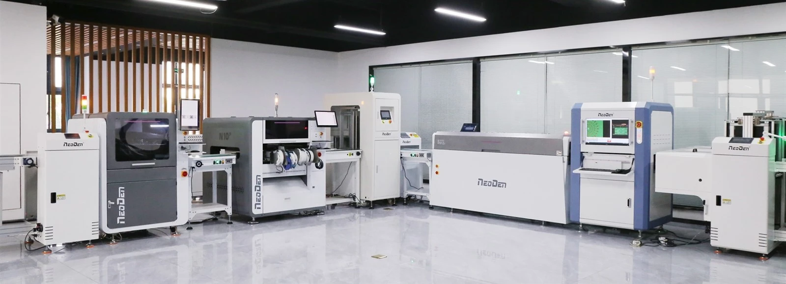
Quick facts about NeoDen
- Established in 2010, 200 + employees, 27000+ Sq.m. factory.
- NeoDen Products:Different Series PnP machines, NeoDen YY1, NeoDen4 ,NeoDen5, NeoDen K1830, NeoDen9, NeoDen N10P. Reflow Oven IN Series, as well as complete SMT Line includes all necessary SMT equipment.
- Successful 10000+ customers across the globe.
- 40+ Global Agents covered in Asia, Europe, America, Oceania and Africa.
- R&D Center: 3 R&D departments with 25+ professional R&D engineers.
- Listed with CE and got 70+ patents.
- 30+ quality control and technical support engineers, 15+ senior international sales, for timely customer responding within 8 hours, and professional solutions providing within 24 hours.