



Introduction
In the PCBA manufacturing industry, "testing" is not the final step in the process, but rather the central quality control thread that runs through the entire manufacturing process. From the initial placement by the SMT placement machine to final shipment, a PCBA typically undergoes a multi-tiered, multi-dimensional inspection system. While the depth of testing varies across different application areas (consumer electronics, automotive electronics, medical devices), the overall structure remains highly consistent. What customers care about is not "whether testing is performed," but "whether the testing chain is complete."
Incoming Materials and Pre-SMT Basic Inspections
In the PCBA manufacturing process, testing does not begin only after soldering is complete, it is already integrated at the materials stage. Before a PCB enters the SMT production line, it must undergo visual inspection and dimensional verification, including board warpage, solder mask integrity, and hole position accuracy. Components also undergo random sampling, with a focus on package specifications, batch consistency, and visual defects. For some high-reliability projects, X-ray inspection or unpackaging verification is added to confirm the consistency of internal structures. The goal of this stage is to prevent "defective components from entering the production line" and reduce the risk of subsequent rework.
AOI Full Inspection After SMT Placement
Once SMT is complete, PCBA manufacturing reaches its first critical testing milestone: AOI (Automated Optical Inspection). AOI is primarily used to inspect post-assembly solder joint quality and component placement accuracy. This includes issues such as misalignment, missing components, polarity errors, bridging, and cold solder joints. On high-end production lines, AOI typically employs multi-angle imaging to enhance the detection of minute defects. This stage constitutes a 100% full inspection and is one of the core steps in ensuring consistent batch quality.
X-Ray Inspection for Hidden Solder Joint Analysis
For invisible solder joint structures such as BGA and QFN, the PCBA manufacturing process must rely on X-ray inspection. X-rays can penetrate component packages to examine the internal solder ball morphology, void rate, and solder continuity. In automotive electronics and telecommunications products, this test is virtually standard. Its purpose is to identify potential risk points where "the surface appears normal but the internal components have failed" at an early stage. If this step is omitted, passing subsequent functional testing does not guarantee that reliability standards have been met.
Functional Testing (FCT) Verifies Electrical Performance
Functional testing is one of the most critical verification steps before a PCBA leaves the factory. FCT (Functional Circuit Test) verifies the electrical functionality of the entire board by simulating actual operating environments. This includes voltage, current, signal transmission, communication interfaces, and control logic. This stage not only verifies "whether the product works" but also confirms "whether it operates as designed." For some products, program burning and online testing are also incorporated to ensure software and hardware compatibility. The FCT results directly determine whether a product qualifies for shipment.
Burn-in Testing to Screen for Early Failures
In high-reliability PCBA manufacturing projects, burn-in testing is a critical process. By continuously operating the board under high-temperature or high-load conditions for a specified duration, it accelerates the exposure of potential defects. Issues such as cold solder joints, material stress instability, or early component failure typically manifest during this stage. Burn-in testing is not standard for all products, but it is widely used in industrial control, automotive electronics, and medical devices. Its core value lies in enhancing the product's long-term stability.
Final Inspection and Visual Verification
After all functional tests are completed, the PCBA products must undergo a final inspection. This stage primarily focuses on visual integrity, marking consistency, solder joint quality, and packaging condition. Test records and batch information are also cross-checked to ensure complete traceability. Some customers also require sampling and retesting to verify the consistency of previous tests. The purpose of the final inspection is to serve as a final risk mitigation measure before shipment.
Significant Variations in Testing Depth Across Products
There is no fixed number of test steps a PCBA must undergo. Rather, this is determined by the application scenario. Consumer products may primarily rely on AOI machine and FCT, while industrial-grade and automotive-grade products typically include additional X-ray inspection and aging tests. Medical and avionics products may even incorporate more stringent environmental stress screening (ESS). The complexity of a PCBA manufacturing test system essentially depends on the product's reliability requirements.
In the PCBA manufacturing industry, testing is not merely an "inspection process," but rather a quality control system that spans the entire manufacturing process. From incoming materials to shipment, every test step helps reduce the failure rate.
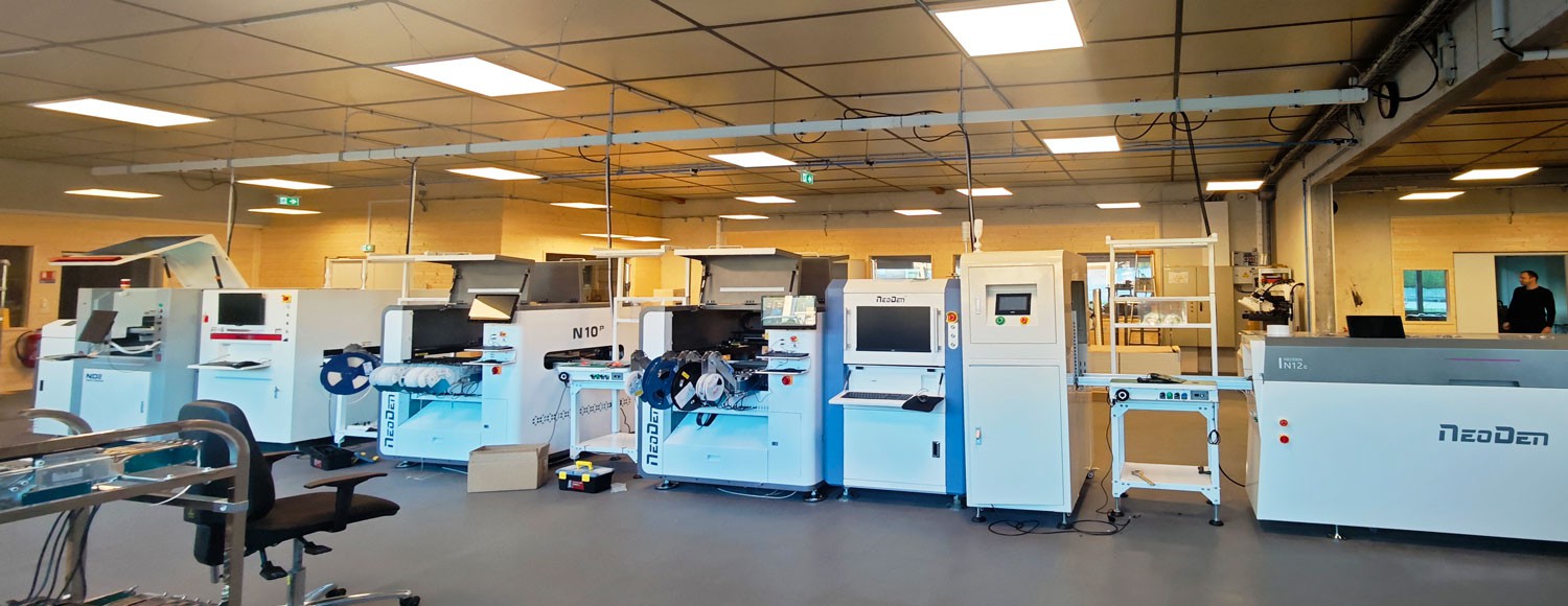
Quick facts about NeoDen
- Established in 2010 with 200+ employees & 27,000+ Sq.m. factory of independent property rights, to ensure the standard management and achieve the most economic effects as well as saving the cost.
- Owned the own machining center, skilled assembler, tester and QC engineers, to ensure the strong abilities for NeoDen machines manufacturing, quality and delivery.
- 40+ global partners covered in Asia, Europe, America, Oceania and Africa, to successfully serve 10000+ users in all of the world, to ensure the better and faster local service and prompt response.
- 3 different R&D teams with total 25+ professional R&D engineers, to ensure the better and more advanced developments and new innovation.
- Skilled and professional english support&service engineers, to ensure the prompt response within 8 hours, solution provides within 24 hours.
- The unique one among all of the Chinese manufacturers who registered and approved CE by TUV NORD.
- NeoDen supplies life-long technical support and service for all of the NeoDen machines, moreover, regular software updates based on the using experiences and actual daily request from the endusers.