



Introduction
In the SMT production process, AOI (Automated Optical Inspection) equipment is a crucial tool for checking the quality of PCB assembly. Using industrial cameras, lighting, and image processing software, AOI can automatically inspect components, solder joints, and other visible features on a PCB, helping production staff identify anomalies such as missing components, misalignment, reversed components, and solder bridges.
How should SMT AOI equipment be used correctly? What steps are involved, from creating a program to analyzing inspection results? This article will introduce the basic operating workflow of AOI equipment in the context of SMT production and, using the NeoDen ND800 SMT AOI Machine as an example, illustrate the application of its features in actual inspections.
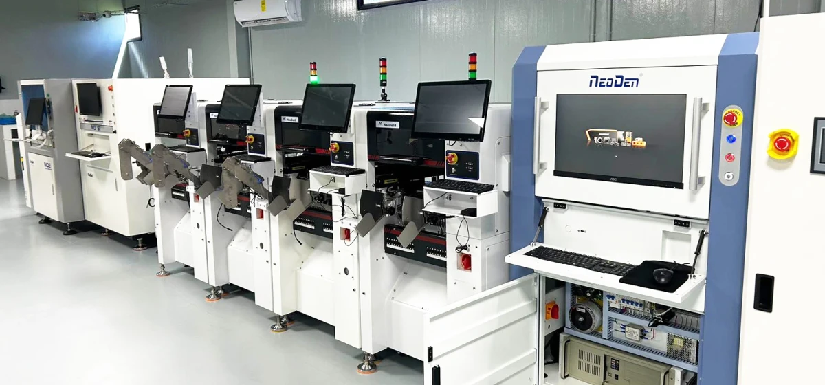
Basic Workflow of SMT AOI Machine
Before using AOI equipment, it is essential to understand its basic workflow.
A typical AOI inspection process includes:
- The PCB enters the machine and is positioned.
- The operator loads the corresponding inspection program.
- Industrial cameras and lighting capture images of the PCB.
- Image processing software analyzes image features.
- The system evaluates the inspection results based on preset standards.
- The machine outputs an "OK" or "NG" result.
- The operator reviews any anomalies and performs rework or process adjustments as needed.
The entire process can be summarized as follows
PCB Positioning → Image Acquisition → Image Analysis → Defect Identification → Result Output → Anomaly Review
It is important to note that AOI inspection results depend on the inspection program, camera and lens configurations, lighting settings, and the actual characteristics of the PCB. Which defects the equipment can identify should be determined based on the actual configuration and the results of sample verification.
What preparations are needed before using SMT AOI equipment?
Before starting the inspection, operators must prepare the PCBs, inspection programs, and relevant production information.
1. Confirm the PCB model and inspection requirements
First, confirm the model, dimensions, thickness, and component layout of the PCBs to be inspected.
If the factory produces multiple types of PCBs, ensure that the currently selected inspection program matches the actual PCB model. Component placement, orientation, and inspection requirements may vary across different PCBs; using the wrong program will affect the inspection results.
At the same time, the objectives of the inspection should be clearly defined, such as:
- Checking for missing components.
- Checking for component misalignment.
- Checking for correct component orientation.
- Checking for solder joint defects.
- Checking for other visible abnormalities on the PCB.
Defining the inspection objectives helps in setting up the appropriate inspection program.
2. Check the Status of the AOI Equipment
Before starting the inspection, confirm that the equipment is in normal operating condition.
Common check items include:
- Whether the camera and lens are clean.
- Whether the lighting is functioning properly.
- Whether the PCB conveyor mechanism is operating normally.
- Whether the equipment's positioning system is functioning properly.
- Whether the inspection software is running normally.
- Whether the connection between the equipment and the production line meets requirements.
If the equipment experiences positioning abnormalities, blurred images, or conveyor malfunctions during the inspection process, troubleshoot the issue first before proceeding with the formal inspection.
3. Verify the Inspection Program
For PCBs with existing programs, call up the corresponding program and verify the board information.
For new products or PCBs with design changes, create or update the inspection program. Program configuration is a critical step in AOI operation and one of the key factors affecting inspection results.
How to Create an SMT AOI Inspection Program?
An AOI inspection program instructs the equipment on which areas to inspect, what inspection standards to apply, and how to identify anomalies.
While the software interfaces vary by AOI brand and model, the basic program creation process typically includes the following steps.
1. Import PCB Design Data
If the AOI software supports CAD data import, you can use the PCB design data to create the inspection program.
CAD data typically includes component coordinates, component part numbers, angles, and material information. By importing this data, operators can reduce manual data entry and lay the foundation for subsequent inspection program setup.
According to the NeoDen ND800 product specifications, this device supports CAD data import as well as both automatic and manual programming.
For factories that frequently switch between PCB models, CAD import and program management capabilities can serve as important considerations during the selection process.
2. Setting Up PCB Alignment and Mark Points
PCB alignment helps the AOI equipment confirm the board's position and orientation.
Operators must configure alignment information-such as mark points-based on the PCB's actual design. During inspection, the equipment uses this alignment information to determine the PCB's position, thereby inspecting the corresponding areas according to the program.
Incorrect alignment settings may cause the inspection area to shift, affecting subsequent image capture and judgment.
3. Setting Inspection Areas
After completing PCB alignment, corresponding inspection areas must be set based on the inspection objectives.
For example:
- Inspecting component areas.
- Inspecting solder joint areas.
- Inspecting specific ICs or connectors.
Setting corresponding inspection programs for areas requiring special attention.
Inspection areas should match the actual PCB layout and inspection objectives. Not all areas require the same inspection method.
4. Configuring Inspection Parameters
AOI software determines whether anomalies exist based on image features and preset standards.
Operators must configure appropriate parameters based on component types, image features, and inspection objectives. Parameter settings should not simply aim for "the stricter, the better," but rather balance defect detection capability with false positive rates.
For new products, it is recommended to validate the program using an actual PCB to verify that the equipment can correctly identify target defects.
How to Use AOI Equipment for PCB Inspection?
Once the program has been set up, the formal inspection process can begin.
1. Load the PCB into the AOI Equipment
Place the PCB onto the equipment's conveyor system and ensure the board meets the equipment's requirements.
For automated SMT production lines, PCBs can be fed into the AOI via a board loader or front-end conveyor system. For standalone equipment, boards must be loaded according to the equipment's operating instructions.
2. Load the appropriate inspection program
The operator selects the appropriate program based on the PCB model and verifies that the program information matches the current board.
Before starting formal production, it is recommended to first conduct a test using a sample board to confirm that the program can correctly identify the PCB and that the inspection areas are set up correctly.
3. Start the automatic inspection
The equipment performs image capture and analysis according to the program settings.
Industrial cameras capture images of the PCBs, and image processing software identifies potential defects based on preset inspection criteria, then outputs the corresponding results.
During the inspection process, operators should monitor the equipment for abnormal alarms, positioning failures, or image acquisition issues.
4. Review the inspection results
The AOI typically outputs an "OK" or "NG" status based on the inspection results.
OK: The current inspection program did not identify any defects exceeding the preset criteria.
NG: The system has identified anomalies that require further verification.
It is important to note that an "OK" result does not mean that all potential defects on the PCB have been detected. AOI inspection results are specific to the current equipment configuration, inspection program, and recognizable image features.
How to Verify NG Results Detected by AOI?
After AOI detects an NG result, the operator must further verify whether the anomaly is a genuine defect.
1. Examine the NG Location and Image
First, examine the location of the anomaly marked by the equipment to confirm exactly which component, solder joint, or inspection area is problematic.
If the software supports zooming in on the anomaly image and comparing it to a reference image, use these features to check the differences between the actual image and the program's standards.
The NeoDen ND800 user manual describes the relevant anomaly review interface, including the NG location, image thumbnails, zoomed-in views, and a comparison between the actual image and the registered image. These features help operators identify anomalies more intuitively.
2. Distinguish Between True Defects and False Positives
Not all "NG" results detected by AOI are necessarily true defects.
For example, reflections on the PCB surface, variations in component appearance, changes in lighting, or inappropriate program parameter settings can all cause the system to flag certain normal features as anomalies.
Operators must make judgments by considering the actual PCB, inspection images, and quality standards.
3. Taking Corrective Actions Based on Anomaly Results
If a genuine defect is confirmed, it should be addressed in accordance with the factory's quality procedures, such as:
- Sending the defective PCB to the rework station.
- Checking the placement machine program and feeder status.
- Inspecting the solder paste printing and reflow soldering processes.
- Recording the defect type and location.
- Adjusting relevant process parameters as needed.
If a false positive is confirmed, the inspection program or relevant parameters should be adjusted in accordance with the equipment operating procedures, followed by revalidation.
The value of AOI lies not only in detecting anomalies but also in helping production personnel pinpoint issues and providing a basis for subsequent quality improvements.

How Can AOI Inspection Data Be Used to Improve SMT Production Quality?
AOI is not only used for quality inspection of individual PCBs but also provides data for production process analysis.
1. Record Defect Types
Production staff can use the inspection results output by the AOI to track the occurrence of different defects.
For example:
- Component misalignment.
- Missing components.
- Components installed in the wrong orientation.
- Solder bridges.
- Insufficient or excessive solder.
- Other identifiable anomalies.
By tracking defect types, the factory can identify which issues are most common in the current production process.
2. Analyzing Defect Trends
If a certain type of defect persists over a period of time, it may indicate that the relevant process has issues requiring further investigation.
For example, component misalignment may be related to the placement program, feeder status, or the placement process; soldering anomalies may require inspection of the solder paste printing, component placement, or reflow soldering processes.
It is important to note that while AOI data can help identify abnormal trends, the root cause cannot be directly determined based on a single type of defect alone. The specific cause still requires evaluation in conjunction with production processes and actual inspections.
3. Using SPC Data to Support Quality Management
SPC (Statistical Process Control) features can help factories record and analyze inspection data.
According to the NeoDen ND800 product specification, this device supports SPC statistical analysis, which can be used to record inspection results and assist in analyzing production quality.
For SMT factories that require continuous monitoring of production quality, inspection data can help quality personnel understand defect distribution and provide a reference for subsequent process improvements.
What are some common issues when using AOI equipment?
1. Why do false positives occur in AOI?
False positives may be related to the inspection program, lighting conditions, image features, PCB surface reflectivity, or parameter settings.
It is recommended to troubleshoot by examining abnormal images, verifying the actual PCB condition, and adjusting program parameters. After adjustments, revalidate using a reference sample to avoid compromising the system's ability to detect actual defects.
2. Why is it necessary to update the program after changing the PCB model?
Component placement, orientation, dimensions, and visual characteristics may vary across different PCBs.
If an old program is used directly, the inspection areas and judgment criteria may no longer be applicable. Therefore, after introducing a new product or making PCB design changes, verify whether the existing program needs to be updated.
3. Can AOI detect all soldering defects?
No.
AOI primarily identifies visible anomalies through optical image recognition. For hidden defects inside solder joints or issues that cannot be reliably determined from surface images, other inspection methods-such as X-ray-should be evaluated based on the inspection objectives.
4. If the AOI inspection result is "OK," does that mean the PCB is definitely defect-free?
Not necessarily.
AOI inspection results depend on equipment configuration, inspection programs, and whether defects can be identified through optical image recognition. For specific products or complex defects, other quality inspection methods and process validation should be integrated to establish a quality control process tailored to your production requirements.
How is the NeoDen ND800 SMT AOI machine applied in production inspection?
The NeoDen ND800 SMT AOI machine is designed to meet the automatic optical inspection needs of SMT production and can be used to inspect anomalies related to solder paste printing, component placement, and certain soldering processes.
According to the product specifications, the ND800 features the following capabilities:
- Supports automatic and manual programming.
- Supports CAD data import.
- Supports multiple image processing methods.
- Supports output of inspection results.
- Supports SPC statistical analysis.
- Equipped with an industrial camera and multi-channel color lighting.
During actual operation, operators can create inspection programs based on PCB type, capture images using the equipment to identify defects, and then use the inspection results to review non-conforming (NG) items and analyze production quality.
For factories planning to purchase AOI equipment, it is recommended to provide actual PCBs, target defects to be inspected, and production line cycle time requirements during the selection phase to confirm whether the equipment configuration meets production needs.
Conclusion
The use of SMT AOI equipment involves more than just starting the machine and running inspections, it also encompasses multiple steps, including program creation, parameter configuration, re-examination of anomalies, and analysis of inspection data. By correctly configuring inspection programs, verifying inspection results using actual PCBs, and reviewing "NG" results, factories can more effectively utilize AOI to identify visible assembly anomalies and support production quality control.
For companies planning or upgrading SMT production lines, selecting AOI equipment that suits their specific PCBs, inspection targets, and production line cycle times is equally important.
Looking for an SMT AOI Solution?
If you are looking for AOI inspection equipment suitable for your production line, contact NeoDen. Provide PCB dimensions, component range, target defects to be inspected, and production requirements so we can further evaluate the appropriate equipment configuration.