


Introduction
In the SMT electronics manufacturing process, reflow soldering is a critical step that determines the quality of PCB solder joints. Engineers typically focus on solder paste printing accuracy, component placement, and joint reliability. However, PCB bending or warpage after reflow soldering is also a significant issue that affects product yield.
So, why do PCBs bend during the reflow soldering process? How can the risk of PCB bending be reduced through process optimization and equipment selection? This article will analyze these issues based on practical SMT production experience and the features of the NeoDen IN6 reflow Oven.
Why Do PCBs Bend During the Reflow Soldering Process?
1. Thermal Stress Caused by Inconsistent Thermal Expansion of PCB Materials
PCBs are not composed of a single material but are formed by laminating multiple different materials, each with distinct thermal expansion characteristics. When a PCB heats up rapidly during the reflow oven soldering process, the different material layers expand to varying degrees. If the heating process is too fast, or if there is a significant temperature difference between the top and bottom surfaces of the PCB, internal stress is likely to develop.
When these stresses cannot be released in a timely manner, the following phenomena may occur:
- Bulging in the center of the PCB.
- Warping at the board edges.
- Overall bending of the PCB.
Therefore, PCB bending is not necessarily a quality issue with the PCB itself, it may also be related to thermal management during the reflow soldering process.
For SMT factories, one of the keys to reducing the risk of PCB warping is to establish a stable and uniform reflow temperature profile.
How does the reflow temperature profile affect PCB warping?
Reflow soldering is not simply a matter of heating the PCB to the melting point of the solder paste, rather, it is a continuous heat treatment process.
A complete reflow profile typically includes:
- Preheating stage
- Soaking stage
- Reflow stage
- Cooling stage
The parameters of each stage affect the thermal stress experienced by the PCB.
1. Excessively fast preheating increases the risk of thermal shock to the PCB
The primary purpose of the preheating stage is to gradually raise the PCB's temperature, thereby:
- Activating the flux.
- Gradually equalizing the temperature across all areas of the PCB.
- Reducing stress caused by sudden temperature changes.
If the heating rate is too fast, the PCB surface may heat up rapidly while the internal temperature remains low.
This temperature gradient can result in:
- Inconsistent expansion rates across different areas of the PCB.
- Additional stress generated within the material.
- An increased likelihood of warping.
Therefore, during SMT process debugging, engineers must not focus solely on peak temperatures but must also pay attention to the entire temperature change process.
The NeoDen IN6 supports adjustable temperature parameters, allowing users to customize zone settings based on different solder pastes and PCB characteristics, thereby helping to establish a more stable reflow profile.
2. Excessively high temperatures during the reflow phase increase the risk of PCB warpage
The reflow phase must reach the solder paste's melting point to ensure reliable solder joints, but excessively high temperatures may result in:
- Increased thermal expansion of the PCB material.
- Greater thermal stress on components.
- A narrower soldering window.
This is particularly true for:
- Thin PCBs.
- PCBs with large copper areas.
- PCBs with high-density components.
Excessively high temperatures can significantly increase the risk of PCB warpage.
The NeoDen IN6's temperature range spans from room temperature to 300°C, meeting the requirements of common lead-free soldering processes. Users can set actual soldering parameters based on the recommended curves provided by their solder paste suppliers.
3. Excessively rapid cooling may generate residual stress
Many production personnel focus more on the heating phase when adjusting reflow soldering parameters, while neglecting the cooling process.
In fact, the cooling phase also affects PCB flatness.
When a PCB rapidly cools from high temperatures to room temperature, different materials contract at different rates, generating internal stress.
If the cooling process is too abrupt:
- The PCB is prone to deformation.
- Internal stress in the solder joints increases.
- Long-term reliability decreases.
Therefore, a comprehensive and reliable reflow soldering process requires attention to the following factors:
- Heating rate.
- Hold time.
- Peak temperature.
- Cooling process.
Apart from the temperature profile, what other factors can cause PCB warpage?
1. PCB Design and Structural Factors
Although reflow soldering is critical for thermal process control, the PCB's own design also influences the risk of warpage.
Common influencing factors include:
- PCB thickness: Thinner PCBs have lower rigidity and are more prone to warpage in high-temperature environments.
- Uneven copper distribution: If the copper area on one side of the PCB is significantly larger than on the other, varying degrees of thermal expansion may occur during heating.
- Uneven component layout: Concentrating large components in a specific area of the PCB can lead to localized differences in thermal capacity.
Therefore, in actual SMT manufacturing, PCB design, material properties, and reflow soldering parameters must be optimized in conjunction.
How does the NeoDen IN6 reduce the risk of PCB bending through its technical design?
Reducing the risk of PCB warping during the reflow soldering process is not simply a matter of lowering the temperature; rather, it requires equipment with more stable thermal management capabilities.

1. Full hot-air convection design to improve PCB heating uniformity
A key cause of PCB warping during reflow soldering is the temperature difference between different areas of the board.
For example:
- Large copper foil areas absorb heat more slowly.
- Large IC component areas have higher thermal capacity.
- Small component areas heat up faster.
If heat distribution within the equipment is uneven, different locations on the same PCB may be at different temperatures, thereby generating thermal stress.
The NeoDen IN6 employs a Full Hot-Air Convection heating method, which uses hot air circulation to evenly transfer heat to the PCB surface.
Compared to traditional methods that rely on radiation from a single heat source, hot-air convection reduces local temperature differences, resulting in a smoother temperature rise for the PCB.
According to the NeoDen IN6 product specifications, the lateral temperature difference within the equipment is less than 2°C, which helps ensure more consistent thermal processing results for the PCB.
For PCBs containing high-density components or complex copper layer structures, this uniform heating capability can effectively reduce the risk of warping caused by local temperature variations.
2. 6 Multi-Zone Design for a Smoother Temperature Ramp
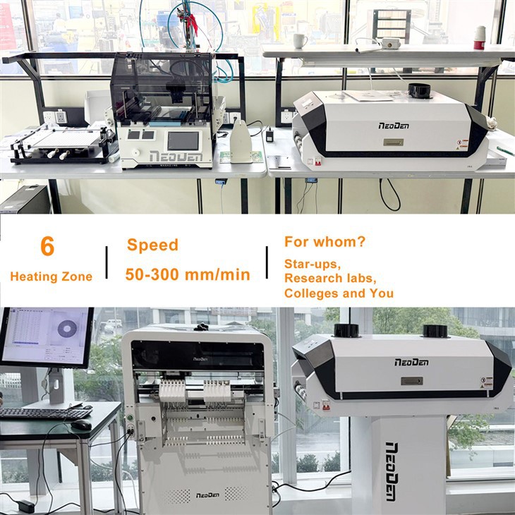
The NeoDen IN6 features a 6-zone design. Through coordinated control of the upper and lower temperature zones, it helps the top and bottom surfaces of the PCB absorb heat more evenly. This is particularly important for reducing PCB warpage.
With multi-zone control, engineers can adjust heating parameters for different stages based on the PCB's characteristics, ensuring the PCB undergoes a smoother temperature ramp.
3. Precise Temperature Control to Reduce Thermal Stress Caused by Temperature Fluctuations
During the SMT production process, temperature stability directly affects the thermal stress state of the PCB.
If significant temperature fluctuations occur in the reflow soldering equipment:
- The PCB may be subjected to repeated temperature changes;
- Different material layers may expand and contract at inconsistent rates;
- Internal residual stress may increase.
The NeoDen IN6 is equipped with high-sensitivity temperature sensors and an intelligent temperature control system, which help the equipment maintain the set temperature more stably.
According to product specifications, the NeoDen IN6 achieves a temperature control accuracy of ±0.2°C, with temperature distribution deviation controlled within ±1°C.
In R&D and small-batch production environments, stable temperature control helps engineers establish more reliable reflow profiles, reducing PCB warpage issues caused by process fluctuations.
4. Real-time Temperature Curve Monitoring for Greater Control Over the PCB Soldering Process
Many PCB bending issues are not caused by equipment malfunctions, but rather by reflow parameters that have not been optimized for the specific PCB.
For example:
With the same temperature settings:
- Thin and thick PCBs exhibit different actual temperature changes.
- PCBs with different component densities absorb heat differently.
- Optimal curves vary depending on the solder paste used.
Therefore, engineers need to measure actual temperatures to understand the PCB's real-time temperature changes.
The NeoDen IN6 supports temperature sensor connections and can capture temperature profiles through actual PCB testing, helping users optimize soldering parameters.
5. Adjustable Conveyor Speed to Improve Process Adaptability for Different PCBs
Different PCBs have varying heat requirements.
For example:
- Thin PCBs: Rapid heating must be avoided;
- Thick PCBs: Sufficient heat transfer must be ensured.
The NeoDen IN6 supports conveyor speed adjustment within a range of 5–30 cm/min, allowing users to adjust the dwell time of the PCB in each temperature zone based on PCB dimensions, thickness, and solder paste type.
This flexibility makes the IN6 suitable not only for single-product applications but also for R&D, small-batch production, and scenarios requiring rapid switching between multiple PCB models.
How Can PCB Bend Be Further Reduced Through SMT Process Optimization?
Although the performance of reflow soldering equipment is crucial, reducing the risk of PCB bend still requires a combination of equipment and process optimization.
1. Adjust Reflow Oven Parameters Based on PCB Characteristics
Different PCBs should use different temperature profiles; a single set of parameters should not be applied to all products.
Engineers need to consider:
- PCB thickness.
- Board type.
- Copper area distribution.
- Component density.
- Solder paste specifications.
When establishing initial parameters, refer to the recommended temperature profiles provided by the solder paste supplier.
The NeoDen IN6 user manual recommends setting reflow soldering temperature parameters based on data provided by the solder paste supplier to ensure the soldering process meets material requirements.
2. Measure temperatures on the actual PCB rather than relying solely on the equipment's displayed temperature
The temperature displayed by the equipment does not fully represent the actual temperature of the PCB.
A more reliable method is:
- Install thermocouples at critical locations on the PCB.
- Obtain the actual temperature profile.
- Analyze temperature differences across different areas.
- Adjust the zone parameters.
This approach helps avoid exposing the PCB to additional thermal stress caused by inaccurate parameter settings.
NeoDen IN6: Helping Companies Establish a Stable PCB Reflow Soldering Process
For electronics R&D teams, small EMS factories, and hardware startups, PCB warpage not only affects product appearance but can also impact solder joint reliability and subsequent assembly.
The NeoDen IN6 helps users establish a more stable and repeatable PCB reflow soldering process.
Additionally, the IN6 features a compact desktop design, measuring 1020 × 507 × 350 mm and weighing approximately 49 kg, making it ideal for R&D laboratories, small-batch production lines, and SMT work environments with limited space.

Conclusion
PCB warping during the reflow soldering process is essentially the result of the combined effects of material properties, temperature changes, and thermal stress.
Through precise temperature control and a stable thermal cycling design, the NeoDen IN6 provides a flexible and reliable reflow soldering solution for PCB prototype development and small-batch manufacturing.
If you are looking for a desktop reflow soldering machine that can improve PCB soldering stability and reduce the risk of reflow warpage, please contact the NeoDen team to obtain detailed specifications for the IN6 and SMT process recommendations tailored to your products.