


Introduction
Extreme application scenarios such as new energy vehicle inverters, on-board chargers (OBCs), and photovoltaic energy storage inverters push the reliability of PCBA manufacturing to new physical limits. When operating at high power, the junction temperature of these products often remains within the high-temperature range of 125°C to 150°C for extended periods. Under the combined effects of continuous thermal and mechanical stresses, lead-free solder alloys undergo a slow and permanent plastic deformation known as "creep." Once creep accumulates to a certain extent, it causes microscopic cracks to form in the solder joints, ultimately leading to fatigue failure. Analyzing the creep mechanism of solder alloys and implementing precise process interventions during PCBA manufacturing are fundamental to ensuring the long-term reliable operation of new energy electronics.
Mechanism of Solder Creep: Grain Boundary Slip in Metals Under High-Temperature Stress
Lead-free solder alloys (such as the commonly used SAC305, a tin-silver-copper alloy containing 3.0% silver and 0.5% copper) have a melting point of approximately 217°C. According to the principles of materials mechanics, when a metal's operating temperature exceeds 50% of its absolute melting point (measured in Kelvin), the creep effect is significantly activated. At 125°C (approximately 398 K), the homologous temperature of SAC305 solder reaches 0.81, far exceeding the creep threshold of 0.5. This means that even under very low stresses-such as the shear stress caused by mismatched coefficients of thermal expansion (CTE) between the PCB and the chip-the tin matrix metal grains within the solder joint will undergo slow mutual slip and atomic diffusion along the grain boundaries. Prolonged high-temperature service leads to grain coarsening within the solder joints, with microscopic voids accumulating at grain boundaries and evolving into macroscopic cracks. This is the fundamental technical cause of poor electrical contact or intermittent open circuits in new energy PCBA assemblies.
Alloy Modification via Trace Element Doping: Enhancing the Grain Boundary Pinning Effect
Since traditional lead-free solders struggle to resist creep damage under prolonged high temperatures, adopting new alloy materials with superior creep resistance is the core strategy for addressing this challenge in current PCBA manufacturing. The production of core boards for new energy applications is gradually incorporating high-reliability solders doped with trace elements (such as bismuth (Bi), antimony (Sb), nickel (Ni), and cobalt (Co)), with Innolot alloys serving as a typical example. By incorporating these trace elements into the tin matrix, a fine and uniformly distributed second-phase dispersion phase is formed within the metal. When creep occurs at solder joints, these hard particles act as "pinning effect" at the grain boundaries, effectively inhibiting metal grain slip and micro-dislocation movement. Experimental data show that in thermal aging tests at 150°C, the tensile strength and high-temperature creep life of Innolot alloys are more than twice that of standard SAC305, providing a robust microstructural barrier for the mainboards of new energy inverters.
Reflow Soldering Cooling Rate Control: Optimizing Initial Grain Size
In addition to the composition of the solder itself, thermodynamic control during the PCBA manufacturing process directly determines the initial microstructure's ability to resist creep. The cooling rate in the reflow soldering process is a key control parameter. Technicians must strictly control the cooling rate during the cooling phase between 3.5°C and 5.5°C per second. Rapid cooling forces the molten metal to solidify quickly, resulting in a fine, dense, and uniformly distributed eutectic microstructure that suppresses the formation of coarse single crystals. Because fine-grained microstructures have more grain boundaries, they provide better mechanical strength at room temperature; furthermore, during the early stages of high-temperature creep, the dense microstructure delays the nucleation and expansion of voids. If the cooling rate is too slow (e.g., below 2.0 °C per second), coarse Ag₃Sn needle-like compounds will precipitate within the solder joints. During subsequent long-term high-temperature service, the areas surrounding these coarse particles are highly prone to becoming stress concentration points and will be the first to induce creep cracking.
Underfill Curing: External Stress Transfer and Dispersion
By restructuring the external stress distribution in the soldered area, it is possible to effectively reduce the creep load borne by the solder alloy and extend the overall service life of the PCBA. For high-temperature, large-size packaged devices carrying high currents on new energy vehicle motherboards (such as IGBT modules and large-size BGAs), manufacturers typically incorporate an underfill process after reflow oven soldering. Using high-precision dispensing machines, high-modulus, low-CTE epoxy resin is injected beneath the chip. Through capillary action, it fills the gaps between the component and the PCB and undergoes thermal curing. The cured resin layer tightly bonds the chip to the board, forming a rigid, integrated unit. When a temperature rise causes CTE mismatch, most of the shear stress is absorbed and dispersed by the outer resin matrix, drastically reducing the physical load applied to the solder paste joints. This delays the onset of the thermal creep phase for the solder alloy at the structural level.
Overcoming the creep challenges associated with solder alloys requires a comprehensive, multi-dimensional approach that encompasses metallurgical selection, oven temperature control, and structural reinforcement.
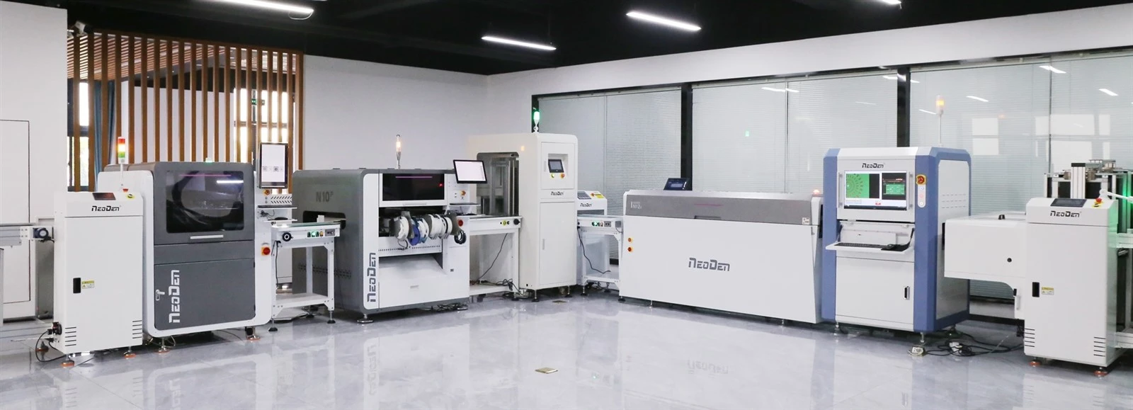
Quick facts about NeoDen
- Established in 2010, 200 + employees, 27000+ Sq.m. factory.
- NeoDen Products:Different Series PnP machines, NeoDen YY1, NeoDen4 ,NeoDen5, NeoDen K1830, NeoDen9, NeoDen N10P. Reflow Oven IN Series, as well as complete SMT Line includes all necessary SMT equipment.
- Successful 10000+ customers across the globe.
- 40+ Global Agents covered in Asia, Europe, America, Oceania and Africa.
- R&D Center: 3 R&D departments with 25+ professional R&D engineers.
- Listed with CE and got 70+ patents.
- 30+ quality control and technical support engineers, 15+ senior international sales, for timely customer responding within 8 hours, and professional solutions providing within 24 hours.