



Introduction
In the PCBA manufacturing industry, pre-shipment testing is the critical checkpoint for maintaining quality standards. However, even after undergoing multiple rounds of inspection, many complex electronic products still exhibit serious issues-such as occasional system crashes and signal distortion-once they reach the customer. Looking at the underlying logic, this is often not due to insufficiently advanced SMT production line testing equipment, but rather a lack of Design for Testability (DFT) during the circuit design phase, which leaves a large number of circuit traces and components in the blind spots of testing equipment. To maximize test coverage, DFT design must be established as a mandatory standard early in the R&D process to thoroughly intercept hidden manufacturing defects before shipment.
Deconstructing Test Coverage: The Physical Matrix of Multidimensional Inspection Technologies
The quality of PCBA testing cannot be judged solely by the results of a single piece of equipment; rather, it requires a matrix-based combination of the coverage ranges provided by different inspection methods. The mainstream inspection chain for PCBA manufacturing consists of Automated Optical Inspection (AOI), Automated X-ray Inspection (AXI), In-Circuit Testing (ICT), and Functional Testing (FCT). AOI and AXI focus on physical appearance characteristics, capable of detecting over 95% of component misalignment, solder deficiency, solder bridging, and internal voids in BGAs at the geometric level. ICT, on the other hand, uses physical probes to contact test points, quantitatively measuring electrical parameter errors in components such as resistors, capacitors, and inductors, and detecting open-circuit and short-circuit defects. FCT simulates the end-user operating environment to perform dynamic functional verification of the entire board through input and output testing. The core objective of DFT design is to ensure that ICT and FCT equipment can unimpeded acquire signals from critical nodes by strategically placing test points during the schematic and PCB layout stages, thereby maximizing comprehensive test coverage to over 98%.
Rigid DFT Specifications at the PCB Level: Precise Control of Test Point Physical Parameters
Test points serve as the physical bridge connecting test instruments to the internal circuits of the PCBA. During the PCB layout phase, the dimensions, spacing, and distribution of test points directly determine the difficulty of manufacturing the pin-bed fixtures and the stability of testing in subsequent manufacturing stages. During DFM/DFT reviews, process engineers must establish strict physical constraints for test points. At least one test point must be reserved for each independent network. The diameter of the test pad must be maintained between 0.8 mm and 1.0 mm. Pads that are too small can cause the center to shift when the test probe is pressed down, leading to frequent false positives. The center-to-center spacing between adjacent test points must be at least 1.27 mm (50 mil). If a 1.0 mm (40 mil) spacing is unavoidable, expensive and brittle microprobes must be procured, which significantly increases tooling costs and reduces durability. Furthermore, test points should be 100% concentrated on the back of the PCB to avoid the need for double-sided pin-bed fixtures, thereby simplifying the mechanical structure and minimizing mechanical stress during each test cycle.
Boundary Scan Technology: Overcoming Hidden Dead Zones in High-Density Chips
With the widespread adoption of miniaturized, multi-pin components such as BGAs, QFNs, and PoPs (stacked packaging), the core pins on the underside of chips have long been inaccessible to physical probes. In such cases, boundary scan technology (JTAG) based on the IEEE 1149.1 standard has become an indispensable tool in DFT design. During the schematic design phase, R&D personnel must select digital chips that support boundary scan functionality (such as high-end CPUs, FPGAs, and DSPs). By embedding shift register units along the chip's internal edges, the standard JTAG interface (comprising five signal lines: TCK, TMS, TDI, TDO, and TRST) is routed to a test connector on the edge of the PCB. At the ICT station after PCBA manufacturing is complete, the tester does not need to use physical probes to contact the hundreds of densely packed solder balls on the bottom of the chip. Instead, by injecting serial test vectors through the JTAG interface, it can read the logic states of each pin in reverse. This technology can detect 100% of cold solder joints and microscopic bridging on the bottom of BGAs, as well as internal logic damage within the chip, completely overcoming the physical space limitations of traditional testing.
Hardware-Software Collaborative FCT Design: Improving Diagnostic Accuracy and Closed-Loop Full Data Flow
Functional testing (FCT) serves as the final line of defense for verifying whether a PCBA is fully operational, DFT design at this stage requires deep collaboration between the software architecture and hardware interfaces. On the hardware side, DFT design requires that critical paths-such as core power rails (e.g., 1.2V, 3.3V, 5V), clock sources, and microprocessor reset pins-be brought out via pin headers or test blind vias to facilitate dynamic current and waveform monitoring by the FCT fixture. On the software side, firmware engineers must embed dedicated test modes and self-test algorithms into the MCU or OS code. When the product is connected to the FCT test bench, the test software sends specific commands via a serial port, CAN bus, or Ethernet, prompting the board to sequentially activate each peripheral module for closed-loop communication. Should data packet loss or frequency deviation occur, the system can accurately report the specific failure code and corresponding component part number within 0.5 seconds, marking a leap in quality control from merely "knowing the board is defective" to "precisely pinpointing which component is damaged."
Embedding DFT design into the very DNA of product development is the inevitable path for PCBA manufacturing to achieve lean production and move toward zero-defect delivery.
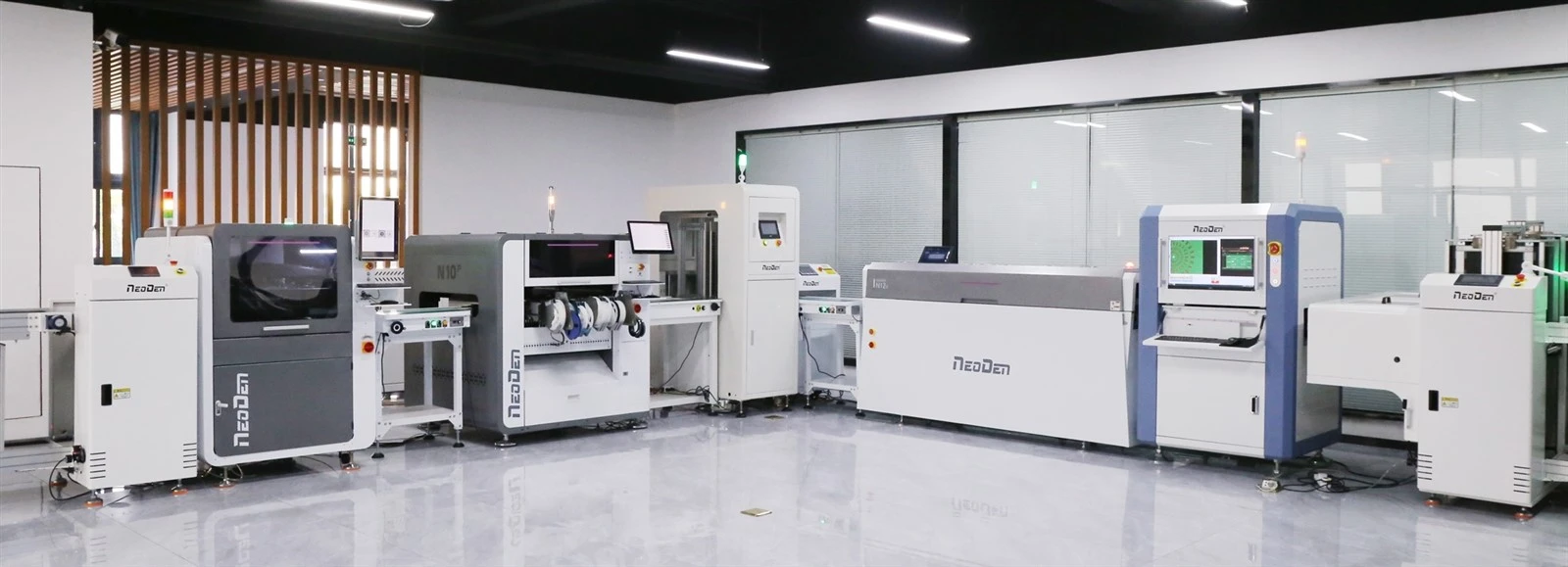
Quick facts about NeoDen
- Established in 2010, 200 + employees, 27000+ Sq.m. factory.
- NeoDen Products:Different Series PnP machines, NeoDen YY1, NeoDen4 ,NeoDen5, NeoDen K1830, NeoDen9, NeoDen N10P. Reflow Oven IN Series, as well as complete SMT Line includes all necessary SMT equipment.
- Successful 10000+ customers across the globe.
- 40+ Global Agents covered in Asia, Europe, America, Oceania and Africa.
- R&D Center: 3 R&D departments with 25+ professional R&D engineers.
- Listed with CE and got 70+ patents.
- 30+ quality control and technical support engineers, 15+ senior international sales, for timely customer responding within 8 hours, and professional solutions providing within 24 hours.