



Introduction
In high-end PCBA manufacturing and design, engineers often emphasize one key principle: high-speed and sensitive signals should be routed on inner layers whenever possible. Many people new to PCB design tend to interpret this practice simply as a means of "mitigating interference," but in reality, the significance of inner-layer routing extends far beyond EMI control. For modern high-density PCBA manufacturing, routing sensitive signals on inner layers is essentially a comprehensive physical protection strategy. Especially as the complexity of high-speed communications, industrial control, and automotive electronics continues to increase, the risks associated with outer-layer routing are no longer limited to signal noise issues but also involve reliability, stability, and long-term environmental adaptability. Therefore, in an increasing number of high-reliability PCBA manufacturing projects, routing core signals on inner layers has become a fundamental design principle.
Outer-layer Traces Are Naturally Exposed to Complex Environments
Once PCBA manufacturing is complete, the outer-layer traces of the PCB are directly exposed to the air and the external environment. Even when the PCB surface is covered by a solder mask, the traces may still be affected by moisture, contaminants, mechanical friction, and static electricity. Particularly in industrial equipment, outdoor terminals, and high-humidity environments, ionic contamination in the air, condensation, and even dust particles can interfere with sensitive outer-layer signals. In contrast, inner-layer traces are naturally enclosed by the PCB substrate, forming a physical isolation barrier. This structure significantly reduces the direct impact of the external environment on sensitive signals.
Inner-layer routing provides a more stable reference plane
In PCBA design and manufacturing, signal stability largely depends on the integrity of the return path. If sensitive signals are routed directly on the outer layers, their reference plane is easily affected by ground copper notches, component placement, and surrounding traces. In contrast, inner-layer traces can typically run adjacent to an intact GND layer or power layer. This not only shortens the return path but also ensures more stable impedance. For DDR, high-speed differential, and RF PCBA manufacturing projects, the advantages of this structure are particularly evident. Many high-speed signal issues are not fundamentally caused by "too high a frequency," but rather by uncontrolled return paths resulting from a discontinuous reference plane.
Outer-layer traces are more susceptible to mechanical damage
During actual PCBA manufacturing and subsequent assembly processes, the PCB surface is subjected to frequent handling. Activities such as panel separation, testing, assembly, repair, and transportation all increase the risk of damage to outer-layer traces. This is particularly true for high-density PCBs, where fine-pitch trace spacing is becoming increasingly narrow. If sensitive signals are routed directly on outer layers, even minor scratches, solder residue, or contact with tools can compromise trace stability. In contrast, inner-layer traces-being embedded within the PCB-are not directly exposed to mechanical handling, resulting in higher long-term reliability. This is a key reason why many military and automotive PCBA manufacturing projects emphasize routing critical traces on inner layers.
Inner-layer Structures Offer Greater Advantages for EMI Control
In the PCBA manufacturing field, EMI issues have long been a major challenge in high-speed design. Because outer-layer traces are directly exposed, they are more prone to becoming sources of electromagnetic radiation. This is particularly true for high-speed clock signals, RF signals, and high-speed differential pairs. If routed directly on the outer layers, their radiated energy is more likely to spread outward. In contrast, inner-layer traces, surrounded by the top and bottom reference layers, form a structure similar to a "shielded cavity." This structure significantly reduces signal leakage. At the same time, it makes it more difficult for external electromagnetic interference to couple directly with inner-layer traces. Therefore, in high-speed PCB design, a large number of core signals are prioritized for placement on inner layers.
Inner-Layer Routing Helps Improve ESD Immunity
Electrostatic discharge (ESD) issues have always been particularly insidious in PCBA manufacturing. Many products perform normally during laboratory testing but may malfunction due to momentary ESD interference during actual field use. If sensitive circuits are located on the PCB surface, ESD energy can more easily couple directly into the signal network. In contrast, because inner-layer circuits are isolated by the PCB substrate, the path for electrostatic discharge is significantly longer. This means that ESD energy is attenuated by the substrate material before it reaches the sensitive signals. Consequently, in industrial control, medical equipment, and communications-related PCBA products, critical control signals are typically not exposed on the outer layers.
High-speed products are becoming increasingly reliant on inner-layer routing
As high-speed interfaces continue to evolve, the requirements for signal integrity in PCBA manufacturing are becoming increasingly stringent. For example, PCIe, USB4, DDR5, and high-speed SerDes circuits demand extremely high impedance continuity. If these signals are routed on outer layers, they are susceptible to variations in the air dielectric, solder mask thickness, and external environmental factors. In contrast, the dielectric structure of inner layers is more stable and offers greater controllability. Therefore, high-speed PCB design typically involves rigorous stack-up planning to prioritize the placement of core differential pairs between inner reference layers. This approach not only improves signal quality but also reduces the risk of subsequent EMC remediation.
Inner-layer routing is not simply a matter of "hiding" the traces
Many people believe that routing sensitive signals on inner layers is solely for the purpose of "hiding the traces." However, from the perspective of actual PCBA manufacturing, it truly addresses system-level stability issues. Aspects such as immunity to interference, physical protection, impedance control, ESD protection, and long-term environmental reliability all benefit as a result. Especially in high-reliability electronic products, inner-layer routing is no longer merely a design optimization but a fundamental requirement for system stability. Many random failures that are difficult to troubleshoot later on actually have their roots in issues planted during the PCB design phase.
In the PCBA manufacturing field, routing sensitive signals on inner layers is not merely a "high-end practice," but rather a reliability design logic born from long-term engineering experience. As electronic products become faster and their structures more complex, physical protection and signal stability can no longer be discussed in isolation.
Company Profile
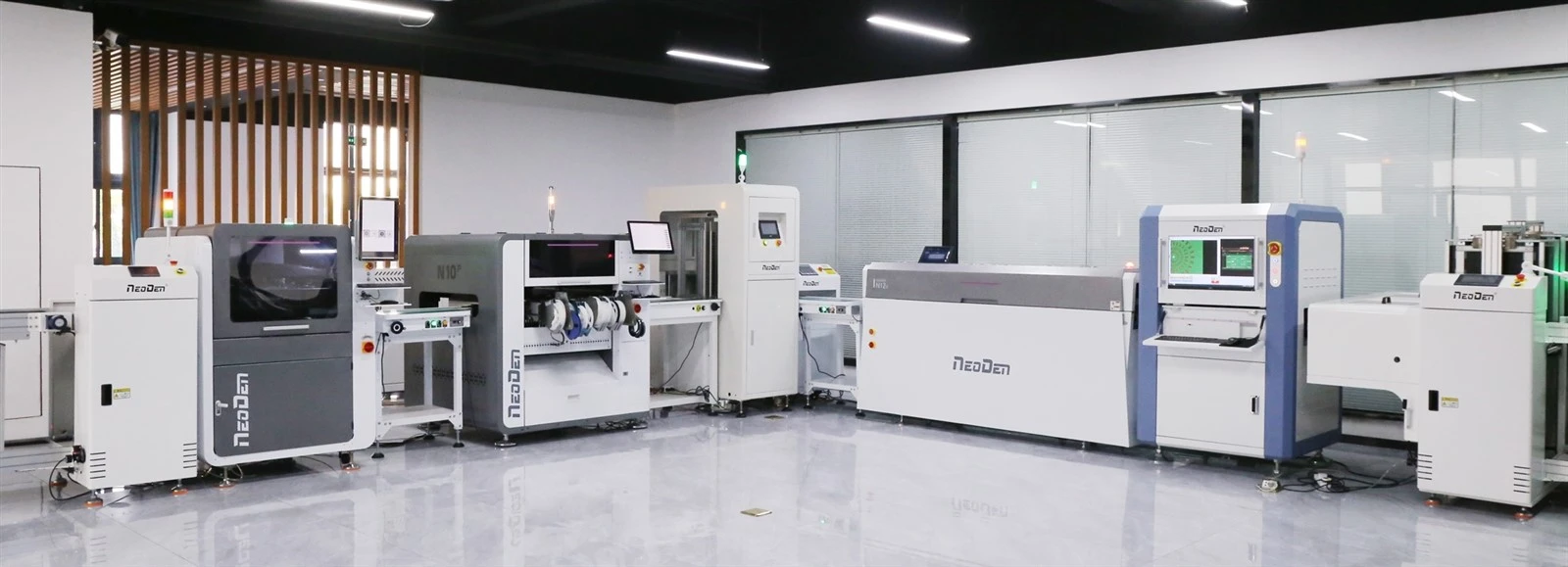
Zhejiang NeoDen Technology Co., Ltd. has been manufacturing and exporting various small pick and place machines since 2010. Taking advantage of our own rich experienced R&D, well trained production, NeoDen wins great reputation from the world wide customers.
with global presence in over 130 countries, the excellent performance, high accuracy and reliability of NeoDen PNP machines make them perfect for R&D, professional prototyping and small to medium batch production. We provide professional solution of one stop SMT equipment.
In our global Ecosystem, we collaborate with our best partners to deliver a more closing sales service, high professional and efficient technical support.
We believe that great people and partners make NeoDen a great company and that our commitment to Innovation, Diversity and Sustainability ensures that SMT automation is accessible to every hobbyist everywhere.