



Introduction
Within the quality management system for PCBA manufacturing, troubleshooting during the functional testing phase has always been the most time-consuming and challenging task for technicians. When a circuit board is powered on and operating, any microscopic manufacturing defect-such as parameter deviations caused by misplaced resistors or capacitors, microscopic bridging hidden beneath ICs, or localized short circuits within the inner layers of multilayer boards-will immediately manifest as abnormal heat dissipation. Traditional point-to-point measurements with a multimeter or waveform capture using an oscilloscope are extremely inefficient when dealing with precision single-board assemblies that often contain thousands of components. The introduction of high-resolution infrared thermal imaging technology-which performs transient temperature field scans of the entire board during the power-on testing phase-converts invisible current anomalies into visual temperature differences, thereby enabling precise screening of localized overheating defects within seconds.
The Physical Nature of Abnormal Overheating During Power-On and the Mechanism of Temperature Rise Failure
When a PCBA is powered on and operating, each component-due to its inherent impedance-experiences a normal temperature rise in accordance with the laws of thermodynamics based on its power dissipation. When deviations occur in the production line process, this thermal equilibrium is instantly disrupted. In PCBA manufacturing, the most common causes of overheating stem from electrical short circuits or reverse breakdown of components. When two adjacent traces form a virtual connection due to a minute short circuit, or when localized solder bridging occurs beneath a large-size BGA, the extremely low resistance of the short-circuit path causes a massive current surge in an instant, resulting in instantaneous heat accumulation at the defect location. Furthermore, in multilayer boards after lamination and soldering, if the electroplated copper layer inside a via contains microscopic burrs or interlayer insulation cracks, high-frequency switching current surges can trigger increased leakage current, causing the thermal resistance in the area surrounding the via to skyrocket. These microscopic physical failures ultimately manifest macroscopically as abnormal localized hot spots that exceed design expectations.
Technical Advantages of Infrared Thermal Imaging and Dynamic Thermal Infrared Panoramic Analysis
Infrared thermal imaging inspection does not rely on contact with any physical probes, it utilizes the physical property that all objects above absolute zero emit infrared radiation to digitally capture the temperature distribution across the board surface. Compared to traditional manual inspection or single-point infrared thermometers, professional-grade 3D infrared thermal imagers are equipped with uncooled focal-plane detectors offering resolutions as high as 640×518 pixels or higher. During the transient period when the PCBA is powered on, the imager can capture dynamic thermal radiation data across the entire board at a rate of over 30 frames per second. The system software converts the collected radiant energy into actual temperature values and generates a color-pseudo-color thermal animation with extremely high spatial resolution on the screen. Even a faint temperature rise of 0.5°C caused by a minor leakage current in a tiny 0201 surface-mount capacitor cannot escape the detector's detection. This panoramic, real-time field-of-view presentation directly visualizes hidden electrical faults.
Digital Threshold Criteria and Temperature Difference (Delta T) Standards for Quality Screening
In the powered-on 100% inspection process for high-performance PCBs-such as those used in automotive electronics and server motherboards-thermal imaging inspection enables fully automated digital rejection by establishing reference thermal images. Engineering departments must set red-line thresholds for each critical physical area of the motherboard within the system software. Under a constant operating current, the system automatically compares the temperature difference between the board under test and the reference board after the same power-on duration. For main power management chips or core processors, the normal operating temperature rise is typically limited to no more than 65°C. If the thermal imager detects that the local maximum surface temperature exceeds 85°C, or exceeds the temperature of the corresponding area on the reference board by more than 10°C, the system immediately triggers a failure determination. For high-frequency differential traces and the areas surrounding power inductors-due to their low thermal capacity-the rejection thresholds are even more stringent; any unexpected sudden temperature rise exceeding 3.5°C will be directly flagged and rejected by the system.
SMT Process Improvement and Defect Traceability Driven by Thermal Imaging Data Chains
Thermal imaging inspection not only serves as a quality control measure at the end of the production line, but the temperature field distribution data it generates also forms the core of the data stream used to adjust SMT placement parameters and upgrade fixture processes on the production line. When a thermal imager frequently reports sudden overheating and boiling at a specific voltage-regulating diode within 3 seconds of power-up for a particular batch of smart control boards, the analysis team can use the geometric center of the thermal image to trace the issue back to earlier stages of the process. By cross-referencing SPI data with the coordinate offset records from the SMT placement machine, technicians can often quickly pinpoint that the stencil aperture size at that location is too large, resulting in excessive solder on the pin after reflow soldering machine and forming a hidden bridge during the reflow process. By reducing the aperture area of that stencil by 20% and conducting another round of mass production and power-on testing, the temperature rise curve in that area will steadily return to the standard green zone. This type of reverse parameter tuning based on thermodynamic characterization establishes a closed-loop quality control system throughout the entire production process.
Precise control of the infrared temperature field during the power-on phase, combined with scientific, digital thermal infrared panoramic imaging to eliminate every latent overheating risk, is a key strategy for maintaining long-term, high-quality delivery in electronics manufacturing.
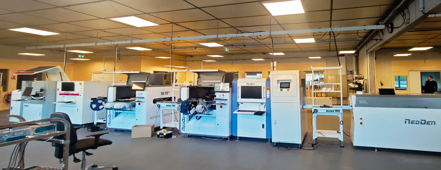
Quick facts about NeoDen
- Established in 2010 with 200+ employees & 27,000+ Sq.m. factory of independent property rights, to ensure the standard management and achieve the most economic effects as well as saving the cost.
- Owned the own machining center, skilled assembler, tester and QC engineers, to ensure the strong abilities for NeoDen machines manufacturing, quality and delivery.
- 40+ global partners covered in Asia, Europe, America, Oceania and Africa, to successfully serve 10000+ users in all of the world, to ensure the better and faster local service and prompt response.
- 3 different R&D teams with total 25+ professional R&D engineers, to ensure the better and more advanced developments and new innovation.
- Skilled and professional english support&service engineers, to ensure the prompt response within 8 hours, solution provides within 24 hours.
- The unique one among all of the Chinese manufacturers who registered and approved CE by TUV NORD.
- NeoDen supplies life-long technical support and service for all of the NeoDen machines, moreover, regular software updates based on the using experiences and actual daily request from the endusers.