



Introduction
In the SMT production process, even when solder paste printing and component placement equipment are operating normally, PCBs may still exhibit component misalignment, missed placements, solder bridges, or other assembly defects. If these issues are not detected in a timely manner, they can increase rework costs and impact subsequent production and product quality.
So, what is SMT AOI equipment? What defects can it detect? Where should it be installed on the SMT production line?
This article will explain the working principles of SMT AOI machine, its primary inspection functions, installation locations, and key factors to consider when selecting AOI equipment. It will also illustrate its application in actual production using the NeoDen ND800 as an example.
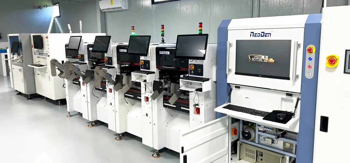
What Is SMT AOI Equipment?
AOI stands for Automated Optical Inspection. SMT AOI equipment is primarily used to inspect for visible defects during the PCB assembly process, assisting production personnel in determining whether products meet preset quality standards.
Compared to methods that rely entirely on manual visual inspection, AOI can automatically capture images, analyze inspection results, and mark locations requiring further verification according to preset programs. It can also save inspection data to serve as a reference for quality analysis.
A typical AOI system usually consists of the following components:
- Industrial cameras and lenses: Capture images of the PCB and components.
- Lighting system: Provides appropriate illumination to enhance image contrast between different surface features.
- Motion and conveyance system: Positions the PCB and completes image capture according to the inspection program.
- Image processing software: Analyzes image features and compares actual results with preset standards.
- Data management system: Records inspection results to support defect tracking and production quality analysis.
These systems work together to perform image capture, defect identification, and the output of inspection results.
How does SMT AOI equipment work?
The core operating principle of AOI is to identify features on a PCB that do not meet preset standards through optical imaging and image analysis. A typical inspection process includes the following steps.
1. The PCB enters the inspection area
The PCB enters the AOI equipment via a conveyor system and is positioned according to the equipment's requirements. The operator loads the corresponding inspection program, and the system determines the inspection area and evaluation criteria based on the PCB model and program settings.
For high-variety, low-volume production, program management and changeover operations are also factors to consider when selecting equipment.
2. Camera and lighting capture images
An industrial camera captures images of the PCB with the assistance of lighting. Different illumination methods can highlight component contours, solder joint surfaces, and other visible features.
Camera pixel count, lens resolution, illumination method, and field of view all affect the final image quality. It is important to note that a higher pixel count does not necessarily mean that all defects can be identified more reliably; the optical system and inspection algorithms must work together to meet actual inspection requirements.
3. Software Analyzes Images and Identifies Anomalies
AOI software uses methods such as color analysis, grayscale processing, and image contrast to determine whether component position, orientation, shape, and solder joint appearance meet preset standards.
Taking the NeoDen ND800 as an example, the user manual lists image processing methods such as machine learning, color calculation, color extraction, grayscale processing, and image contrast. The system can flag anomalies based on the inspection program and output corresponding inspection results.
4. Outputting Inspection Results and Recording Data
Upon completion of the inspection, the equipment outputs an "OK" or "NG" result based on the settings. For PCBs marked as "NG," operators can further examine the location of the anomaly and the corresponding image to confirm whether it is a genuine defect or a false positive.
Therefore, AOI is not merely "taking a photo"; rather, it combines image acquisition, program-based judgment, and result recording to help factories establish a more systematic visual inspection process.
What defects can SMT AOI equipment detect?
The actual inspection capabilities of AOI depend on the equipment configuration, inspection locations, program settings, and whether the defects themselves can be identified through optical image recognition. Common inspection items primarily include the following categories.
1. Solder paste printing defects
After solder paste printing, AOI can identify certain visible anomalies based on images, such as:
- Solder paste misalignment.
- Insufficient or excessive solder paste.
- Solder paste bridging.
- Solder paste contamination.
- Abnormalities in the printed surface.
However, if the production objective is to measure specific parameters such as solder paste volume, height, and area, SPI (Solder Paste Inspection) equipment should generally be prioritized. The inspection methods and primary purposes of AOI and SPI are not entirely the same.
2. Component Placement Defects
After component placement, AOI can inspect for a variety of common assembly anomalies, including:
- Missing or incorrect components.
- Component positional misalignment.
- Skewed components.
- Components installed upside down.
- Anomalies such as tombstoning or components standing on their sides.
Timely identification of these issues helps production personnel review the placement program, feeder status, and placement process, thereby reducing the risk of defects entering subsequent processes.
3. Soldering Defects
After reflow soldering, AOI can identify certain soldering anomalies-such as solder bridges, insufficient solder, excess solder, cold joints, or solder balls-by examining the appearance of solder joints and related image features.
However, not all soldering defects can be reliably identified through standard optical inspection. For hidden solder joints, such as those in BGAs, if it is necessary to inspect the internal connections of the solder joints, inspection methods such as X-ray are typically required based on product specifications.
4. PCB and DIP-Related Anomalies
Depending on the equipment's inspection capabilities and program settings, AOI can also be used to identify certain surface anomalies on PCBs, as well as issues with DIP components such as missing parts, damage, misalignment, or incorrect orientation.
Therefore, when purchasing an AOI system, one should not merely ask, "How many types of defects can the equipment detect?" but should also provide actual PCB samples, target defects, and process information to confirm whether the relevant anomalies can be reliably identified.
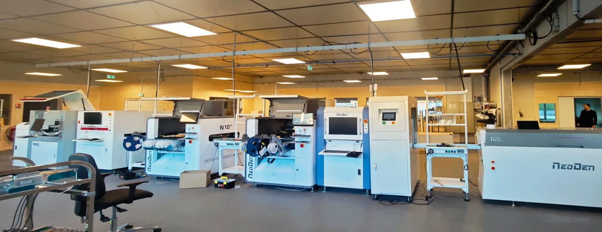
Where Should AOI Be Installed on an SMT Production Line?
The installation location of AOI depends on the production stage at which the factory wishes to detect issues. Common configurations include the following.
1. After Solder Paste Printing
Placing AOI after the solder paste printer allows for the inspection of certain printing anomalies. If the primary objective is to quantitatively assess solder paste deposition quality, the use of SPI should be considered.
2. After SMT machine, before reflow soldering
Installing an AOI after the placement machine allows for the inspection of missing, misaligned, reversed, or tilted components. This enables the detection of some placement issues before reflow soldering, but it cannot replace post-reflow solder joint inspection.
3. After reflow soldering
After reflow soldering is one of the common locations for AOI inspection. The equipment can detect certain component placement and solder joint appearance anomalies, helping the factory evaluate PCB quality after soldering.
A relatively complete SMT production line can adopt the following layout:
PCB Loader → Solder Paste Printer → SPI → Pick-and-Place Machine → Reflow Oven → AOI → PCB Unloader
The actual combination of equipment should be determined based on production volume, product type, inspection objectives, and factory space; not every production line needs to be equipped with all of these devices.
What is the difference between AOI and SPI?
Both AOI and SPI are inspection devices used in SMT production, but they focus on different stages of the process.
| Comparison | SPI | AOI |
| Full Name | Solder Paste Inspection | Automated Optical Inspection |
| Primary Inspection Targets | Printed solder paste | Components, solder joints, and other visible features |
| Common Inspection Items | Solder paste area, volume, height, and misalignment, etc. | Missing components, misalignment, reversed placement, bridging, and certain soldering defects |
| Common Installation Location | After the solder paste printer | After printing, after component placement, or after reflow soldering, depending on the inspection objectives |
| Primary Purpose | To evaluate solder paste printing quality | To inspect assembly and certain soldering quality |
For SMT factories seeking to strengthen process quality control, SPI and AOI can complement each other: SPI focuses on solder paste printing, while AOI focuses on component assembly and visible soldering defects. Whether to configure both systems simultaneously should be determined based on product quality requirements and the production process.
How to Select the Right SMT AOI Equipment?
When selecting an AOI system, it is recommended to evaluate the following aspects.
1. Confirm PCB Dimensions and Component Range
First, verify the PCB's maximum and minimum dimensions, board thickness, curvature, and the minimum component and IC pin pitch. The equipment must be capable of accommodating the actual PCBs and meeting the detection requirements for target defects.
2. Evaluate Cameras, Lenses, and Lighting
Camera resolution, lens parameters, and lighting configurations must be matched to the inspection targets. For fine components or complex solder joints, verify imaging quality and defect recognition capabilities using actual samples rather than simply comparing camera pixel counts.
3. Match the Production Cycle
Confirm whether the AOI's actual full-board inspection time meets production line requirements. The equipment's movement speed is not equivalent to the full-board inspection speed; PCB area, number of inspection points, program complexity, and image processing time all affect actual throughput.
4. Review Programming and Data Management Features
If the factory needs to switch between PCB models frequently, focus on features such as automatic programming, CAD data import, and component libraries. If defect trend analysis is required, confirm whether the equipment supports inspection data logging, SPC statistics, and review of anomalous images.
5. Validate with Actual PCBs
Before purchasing, it is recommended to provide the supplier with actual PCBs and specific defect examples to evaluate inspection performance, false positive rates, per-board inspection time, and the workload involved in program setup. This provides more valuable insight than making a decision based solely on a spec sheet.
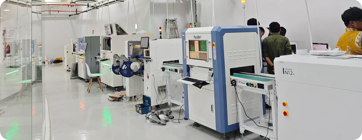
What are the features of the NeoDen ND800 SMT AOI machine?
The NeoDen ND800 SMT AOI machine is designed to meet the automatic optical inspection needs of SMT production and can be used for applications such as solder paste printing, component placement, and quality inspection of certain solder joints. Specific inspection items depend on the equipment configuration, installation location, and inspection program.
According to the product documentation, the ND800 features the following:
- Industrial Camera Configuration: Comes standard with a 5MP full-color high-speed industrial digital camera, with an optional 20MP configuration available.
- Multi-Channel Color Lighting: A ring-shaped, three-dimensional multi-channel lighting system that supports various lighting combination options.
- Image Processing Capabilities: Supports machine learning, color calculation, color extraction, grayscale processing, and image contrast adjustment.
- Programming and Data Management: Supports automatic and manual programming, CAD data import, and SPC statistical analysis.
- PCB Compatibility Range: The product documentation lists a PCB size range of 50 × 50 mm to 400 × 360 mm, with a board thickness range of 0.3–5 mm.
The above specifications are subject to the latest technical documentation for the current sales configuration. In particular, for the detection capabilities of the smallest components, fine-pitch ICs, and specific defects, verification using actual PCB samples is recommended.
For factories planning an SMT inspection process, the ND800 can be considered as one of the candidate systems. The final configuration should be determined based on PCB dimensions, inspection objectives, production cycle times, and data management requirements.
FAQ
Q1. What is the primary use of AOI equipment?
AOI equipment uses cameras, lighting, and image processing software to automatically inspect components, solder joints, and other visible features on PCBs, helping to identify anomalies such as missing components, misalignment, reversed placement, and bridging.
Q2. Can AOI completely replace manual visual inspection?
It cannot be simply assumed that AOI can completely replace manual inspection. While AOI can automatically perform repetitive inspections and flag anomalies, the verification of false positives, assessment of complex defects, decisions regarding rework, and process improvements may still require the involvement of specialized personnel.
Q3. Should AOI be installed before or after the reflow soldering process?
It depends on the inspection objectives. Pre-reflow AOI is primarily used to inspect certain component placement anomalies; post-reflow AOI can inspect certain soldering and placement appearance anomalies. Factories can also combine different inspection locations based on quality control requirements.
Q4. What determines the price of SMT AOI equipment?
AOI pricing is typically influenced by factors such as camera and lens configurations, lighting, PCB inspection range, software functionality, automation level, and service requirements. We recommend providing PCB parameters and inspection requirements to obtain a quote for the appropriate configuration from suppliers.
Conclusion
SMT AOI equipment uses automatic optical inspection to help factories identify visible defects during the PCB assembly process and provides data support for quality tracking and process analysis. When selecting equipment, you should comprehensively consider inspection objectives, PCB size, optical systems, production line cycle time, software features, and equipment integration requirements, rather than comparing a single parameter alone.
Ready to choose an AOI system for your SMT production line?
Provide the NeoDen team with your PCB dimensions, component range, target defects, and production line cycle time, and we can help evaluate the appropriate equipment configuration based on your actual needs.