



Introduction
During operation, the onboard control mainboards of rail transit vehicles are subjected to continuous low-frequency vibrations and sudden high-acceleration shocks. Under these high-vibration conditions, the most critical threat facing PCBA manufacturing is brittle fracture of solder joints. This type of fracture typically occurs at the intermetallic compound (IMC) interface between lead-free solder joints and PCB pads. It is characterized by sudden onset without warning and can easily lead to signal interruptions or control failures on trains. To improve the vibration fatigue life of rail transit mainboards, the fundamental solution lies in optimizing the composition of the solder alloy from a micro-metallurgical perspective.
Mechanism of Brittle Fracture Under Vibration Stress: Stress Concentration in the IMC Layer
During the reflow soldering stage of PCBA manufacturing, the tin in conventional lead-free solder reacts with the copper on the PCB surface, inevitably forming a layer of intermetallic compounds (IMC). Although this eutectic structure serves as a bond for a strong mechanical connection, it is inherently a brittle material. During the service life of rail transit equipment, complex alternating mechanical stresses continuously act on the components and the substrate. Due to significant differences in the coefficients of thermal expansion (CTE) and elastic moduli between the PCB substrate (FR-4) and ceramic components or silicon chips, the mechanical deformation stresses generated by vibration become highly concentrated at the IMC interface, which is only a few micrometers thick. When the accumulated shear stress exceeds the bond strength at the grain boundaries, cracks rapidly initiate and propagate laterally within the IMC or at its interface with the copper pad, causing instantaneous brittle delamination of the solder joint.
Adding Trace Amounts of Bismuth and Antimony: Strengthening the Tin Matrix and Refining the Grain Structure
To counteract high-intensity mechanical vibrations, improving the microstructure of the solder alloy and slowing the rate of crack propagation are the primary objectives in optimizing the alloy composition. In the surface-mount manufacturing of high-power mainboards for rail transit, new high-reliability alloys-based on traditional tin-silver-copper (SAC) but doped with trace amounts of bismuth (Bi) and Stibium (Sb) -are now widely used. The incorporation of bismuth enables solid solution strengthening, significantly enhancing the yield strength of the solder matrix itself. Meanwhile, the addition of antimony slows the rate of grain coarsening under high-temperature and stress conditions, maintaining a fine-grained microstructure. Finer grains result in a substantial increase in the number of grain boundaries. When vibration shock waves propagate into the solder joint, these numerous grain boundaries effectively disperse and absorb energy, forcing microcracks to continuously change their direction of propagation and lengthening their path to penetration, thereby extending the dynamic fatigue life of the solder joint by more than 1.5 times.
Synergistic Effect of Trace Amounts of Nickel and Cobalt: Modifying IMC Morphology and Thickness
While controlling the strength of the crystalline matrix, it is essential to directly "thin" and modify the microstructure of the IMC layer-the site where brittle fracture occurs. By introducing trace amounts of nickel (Ni) and cobalt (Co)-approximately 0.05%-into the solder paste alloy, the growth kinetics of interfacial intermetallic compounds during the reflow process can be significantly altered. Nickel can displace a portion of the copper, transforming the originally coarse, fan-shaped, and unevenly thick eutectic layer into a smoother, denser, and uniformly thick composite crystal structure. Cobalt, on the other hand, effectively suppresses the uncontrolled growth of a poor-quality brittle layer caused by secondary diffusion triggered by temperature rises during the PCBA's subsequent long-term service. Strictly controlling the overall thickness of the IMC layer within an optimal range can significantly reduce stress concentration at the interface and eliminate the conditions conducive to brittle fracture.
Combined with Surface Treatment Technology: Creating a Metallurgical Interface That Balances Rigidity and Flexibility
The advantages of the solder composition must be perfectly matched, both physically and chemically, with the surface finish of the PCB pads to achieve optimal vibration resistance. For high-vibration rail transit motherboards, electroplated nickel-gold (ENIG) surface finishes-which can easily cause black pad phenomena and brittle fracture of phosphorus-rich layers-are generally not recommended. Instead, organic solder preservative (OSP) or electronic-grade immersion silver (Im-Ag) are preferred. The OSP surface treatment allows the formulated high-performance solder to come into direct contact with bare copper, forming a pure copper-tin eutectic layer during reflow soldering and preventing lattice distortion at the interface caused by the introduction of third-party impurity metal atoms. Under this metallurgical interface, combined with an appropriate thickness of conformal coating or localized underfill, a defense mechanism that balances rigidity and flexibility is formed-where the external structure relieves stress and the internal microstructure absorbs energy-thereby completely eliminating the possibility of brittle fracture.
Overcoming the problem of solder joint brittle fracture under high-vibration conditions requires a comprehensive technical approach, ranging from the fine-tuning of microstructural metallurgical composition to the optimization of macroscopic process parameters.
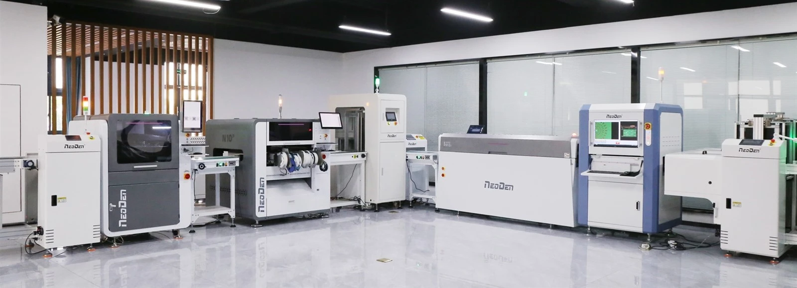
Quick facts about NeoDen
- Established in 2010 with 200+ employees & 27,000+ Sq.m. factory of independent property rights, to ensure the standard management and achieve the most economic effects as well as saving the cost.
- Owned the own machining center, skilled assembler, tester and QC engineers, to ensure the strong abilities for NeoDen machines manufacturing, quality and delivery.
- 40+ global partners covered in Asia, Europe, America, Oceania and Africa, to successfully serve 10000+ users in all of the world, to ensure the better and faster local service and prompt response.
- 3 different R&D teams with total 25+ professional R&D engineers, to ensure the better and more advanced developments and new innovation.
- Skilled and professional english support&service engineers, to ensure the prompt response within 8 hours, solution provides within 24 hours.
- The unique one among all of the Chinese manufacturers who registered and approved CE by TUV NORD.
- NeoDen supplies life-long technical support and service for all of the NeoDen machines, moreover, regular software updates based on the using experiences and actual daily request from the endusers.